


 The Right Approach: I Hear the Train A Comin'
 It’s Only Common Sense: OCCAM—the Time Is Now
 Marcy's Musings: The Growing Industry
Landscapes Give Latitude to 2-D Material Designers
August 10, 2017 | Rice UniversityEstimated reading time: 4 minutes
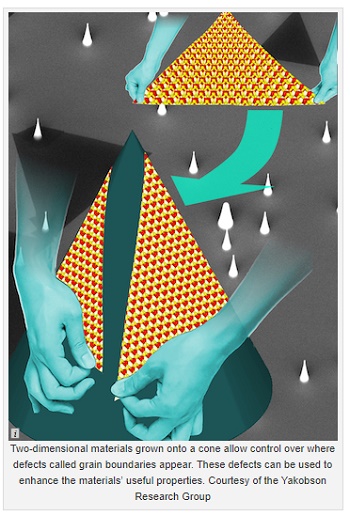
Rice University researchers have learned to manipulate two-dimensional materials to design in defects that enhance the materials’ properties.
Two-dimensional materials grown onto a cone allow control over where defects called grain boundaries appear. These defects can be used to enhance the materials’ useful properties. Courtesy of the Yakobson Research Group
The Rice lab of theoretical physicist Boris Yakobson and colleagues at Oak Ridge National Laboratory are combining theory and experimentation to prove it’s possible to give 2-D materials specific defects, especially atomic-scale seams called grain boundaries. These boundaries may be used to enhance the materials’ electronic, magnetic, mechanical, catalytic and optical properties.
The key is introducing curvature to the landscape that constrains the way defects propagate. The researchers call this “tilt grain boundary topology,” and they achieve it by growing their materials onto a topographically curved substrate — in this case, a cone. The angle of the cone dictates if, what kind and where the boundaries appear.
Grain boundaries are the borders that appear in a material where edges meet in a mismatch. These boundaries are a series of defects; for example, when two sheets of hexagonal graphene meet at an angle, the carbon atoms compensate for it by forming nonhexagonal (five- or seven-member) rings.
Yakobson and his team have already demonstrated that these boundaries can be electronically significant. They can, for instance, turn perfectly conducting graphene into a semiconductor. In some cases, the boundary itself may be a conductive subnanoscale wire or take on magnetic properties.
A theoretical model at left, created at Rice University, shows a triangular flake of tungsten disulfide grown around a cone that forces the creation of a grain boundary at a specific angle. The Rice researchers showed the width of the cone could be used to determine the placement of the boundary, and scientists at Oak Ridge National Laboratory proved it when they made the matching material seen in the electron microscope image at right.
A theoretical model at left, created at Rice University, shows a triangular flake of tungsten disulfide grown around a cone that forces the creation of a grain boundary at a specific angle. The Rice researchers showed the width of the cone could be used to determine the placement of the boundary, and scientists at Oak Ridge National Laboratory proved it when they made the matching material seen in the electron microscope image at right. Courtesy of the Yakobson Research Group
But until now researchers had little control over where those boundaries would appear when growing graphene, molybdenum disulfide or other 2-D materials by chemical vapor deposition.
The theory developed at Rice showed growing 2-D material on a cone would force the boundaries to appear in certain places. The width of the cone controlled the placement and, more importantly, the tilt angle, a crucial parameter in tuning the materials’ electronic and magnetic properties, Yakobson said.
Experimental collaborators from Oak Ridge led by co-author David Geohegan provided evidence backing key aspects of the theory. They achieved this by growing tungsten disulfide onto small cones similar to those in Rice’s computer models. The boundaries that appeared in the real materials matched those predicted by theory.
“The nonplanar shape of the substrate forces the 2-D crystal to grow in a curved ‘non-Euclidian’ space,” Yakobson said. “This strains the crystal, which occasionally yields by giving a way to the seams, or grain boundaries. It’s no different from the way a tailor would add a seam to a suit or a dress to fit a curvy customer.”
Modeling cones of different widths also revealed a “magic cone” of 38.9 degrees upon which growing a 2-D material would leave no grain boundary at all.
Researchers at Rice University and Oak Ridge National Laboratory predict and confirmed that two-dimensional materials grown onto a cone allows control over where defects called grain boundaries appear. At left, a Rice model predicts how a grain boundary would form on a steep cone and extend onto a shallow cone. Scientists at Oak Ridge confirmed the prediction when they created the material seen in an electron microscope image at right.
Researchers at Rice University and Oak Ridge National Laboratory predict and confirmed that two-dimensional materials grown onto a cone allows control over where defects called grain boundaries appear. At left, a Rice model predicts how a grain boundary would form on a steep cone and extend onto a shallow cone. Scientists at Oak Ridge confirmed the prediction when they created the material seen in an electron microscope image at right. Click on the image for a larger version. Courtesy of the Yakobson Research Group
The Rice team extended its theory to see what would happen if the cones sat on a plane. They predicted how grain boundaries would form over the entire surface, and again, Oak Ridge experiments confirmed their results.
Yakobson said both the Rice and Oak Ridge teams were working on aspects of the research independently. “It was slow going until we met at a conference in Florida a couple of years back and realized that we should continue together,” he said. “It was certainly gratifying to see how experiments confirmed the models, while sometimes offering important surprises. Now we need to do the additional work to comprehend them as well.”
Rice graduate students Henry Yu and Nitant Gupta are co-lead authors of the paper. Co-authors are former Rice postdoctoral researcher Zhili Hu, now at Nanjing University of Aeronautics and Astronautics, and researchers Kai Wang, Bernadeta Srijanto and Kai Xiao of Oak Ridge National Laboratory. Geohegan is the functional hybrid nanomaterials group leader at Oak Ridge’s Center for Nanophase Materials Sciences. Yakobson is the Karl F. Hasselmann Professor of Materials Science and NanoEngineering and a professor of chemistry.
The U.S. Department of Energy Basic Energy Sciences and its Center for Nanophase Materials Sciences and the Office of Naval Research supported the research.
Share on:


Suggested Items
Real Time with... IPC APEX EXPO 2024: Sustainability in the Industry
04/26/2024 | Real Time with...IPC APEX EXPOGuest Editor Henry Crandall and Chris Nash of Indium Corporation discuss the company's 90th anniversary and its focus on sustainability. They focus on the benefits of sustainable materials, their compatibility, and value propositions. The conversation also highlights how Durafuse LT technology's role in reducing reflow temperatures is leading to significant cost and energy savings. Nash also touches on downstream sustainability efforts such as using recycled materials for packaging.
SMC Korea 2024 to Highlight Semiconductor Materials Trends and Innovations on Industry’s Path to $1 Trillion
04/24/2024 | SEMIWith Korea a major consumer of semiconductor materials and advanced materials a key driver of innovation on the industry’s path to $1 trillion, industry leaders and experts will gather at SMC (Strategic Materials Conference) Korea 2024 on May 29 at the Suwon Convention Center in Gyeonggi-do, South Korea to provide insights into the latest materials developments and trends. Registration is open.
Groundbreaking Ceremony Marks the Beginning of a New Era for Newccess Industrial; The Construction of the MINGXIN Building
04/12/2024 | Newccess IndustrialOn a clear and sunny day in March, the groundbreaking ceremony for the MINGXIN Building took place in Shenzhen, China. This moment marked the official commencement of construction for a project that will reshape the semiconductor materials industry.
The Need for a Holistic Global Sustainability Standard
04/10/2024 | Michael Ford, Aegis SoftwareNo one can deny that the resources of our fragile planet are finite. The environment seems like a third party, subject to constant degradation. We’re acutely aware of the effects of pollution on our climate, and despite our “throw-away” culture, recycling and recovery of materials has remained relatively expensive, even as we use more energy just to survive.
iNEMI Publishes Four Roadmap Topics
04/04/2024 | iNEMIThe International Electronics Manufacturing Initiative (iNEMI) announces the availability of the first roadmap topics in the new iNEMI Roadmap format. Printed circuit boards, sustainable electronics, smart manufacturing, and mmWave materials and test are now available online.