


 The Right Approach: I Hear the Train A Comin'
 It’s Only Common Sense: OCCAM—the Time Is Now
 Marcy's Musings: The Growing Industry
Fewer Defects from a 2D Approach
August 14, 2017 | KAUSTEstimated reading time: 2 minutes
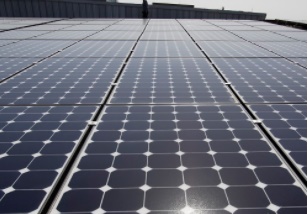
Improving the efficiency of solar cells requires materials free from impurities and structural defects. Scientists across many disciplines at KAUST have shown that 2D organic-inorganic hybrid materials feature far fewer defects than thicker 3D versions.
Modern-day electronics rely on technologies that can develop almost perfect crystals of silicon; flawless to the atomic level. This is crucial because defects and impurities scatter electrons as they flow, which adversely affects the material’s electronic properties.
But hybrid perovskites, an exciting class of electronic material, cannot be constructed using the epitaxial or layer methods developed for silicon. Instead, they are produced using solution-based processes. While this makes them cheaper than silicon, it also makes purity much harder to achieve as defect population and species are sensitive to the processing conditions.
Osman Bakr from the KAUST Solar Center together with colleagues from multiple divisions across KAUST and the University of Toronto, demonstrate that two-dimensional layers of perovskite material can achieve levels of purity much higher than is possible than in their 3D counterpart. “Two-dimensional hybrid perovskites are a subgroup of the big hybrid perovskite family,” explains Wei Peng, lead author and doctoral degree recipient from Bakr’s lab. “They can be derived by inserting large organic cations in three-dimensional perovskite structures.”
Hybrid perovskites are made up of lead and halide (such as iodine) atoms and an organic component. This class of materials in solar cells has already shown ground-breaking potential for energy conversion efficiency while having low production costs and the possibility for being integrated in flexible devices. This combination of qualities makes hybrid perovskites an exciting material for optoelectronic applications.
Peng, Bakr and coworkers created a 2D material made of periodic layers of hybrid perovskites with an organic component of either phenethylammonium or methylammonium. Using a solution-based fabrication method, the layers were placed on a gold electrode so the team could measure the electrical conductivity.
Their measurements indicate that the 2D materials contained three orders of magnitude fewer defects than bulk hybrid perovskites. The team proposes that this reduction is because the large organic cations in the phenethylammonium suppress defect formation during crystallization.
Next, the team demonstrated the potential for their materials for optoelectronic applications by constructing photoconductors with high light detectivity. These results bode well for further advancements in designing and optimizing perovskite solar cells. “A future in-depth study on how the defect formation is suppressed will help our understanding and benefit device performance-targeted materials engineering,” says Peng.
Share on:


Suggested Items
SMC Korea 2024 to Highlight Semiconductor Materials Trends and Innovations on Industry’s Path to $1 Trillion
04/24/2024 | SEMIWith Korea a major consumer of semiconductor materials and advanced materials a key driver of innovation on the industry’s path to $1 trillion, industry leaders and experts will gather at SMC (Strategic Materials Conference) Korea 2024 on May 29 at the Suwon Convention Center in Gyeonggi-do, South Korea to provide insights into the latest materials developments and trends. Registration is open.
Groundbreaking Ceremony Marks the Beginning of a New Era for Newccess Industrial; The Construction of the MINGXIN Building
04/12/2024 | Newccess IndustrialOn a clear and sunny day in March, the groundbreaking ceremony for the MINGXIN Building took place in Shenzhen, China. This moment marked the official commencement of construction for a project that will reshape the semiconductor materials industry.
The Need for a Holistic Global Sustainability Standard
04/10/2024 | Michael Ford, Aegis SoftwareNo one can deny that the resources of our fragile planet are finite. The environment seems like a third party, subject to constant degradation. We’re acutely aware of the effects of pollution on our climate, and despite our “throw-away” culture, recycling and recovery of materials has remained relatively expensive, even as we use more energy just to survive.
iNEMI Publishes Four Roadmap Topics
04/04/2024 | iNEMIThe International Electronics Manufacturing Initiative (iNEMI) announces the availability of the first roadmap topics in the new iNEMI Roadmap format. Printed circuit boards, sustainable electronics, smart manufacturing, and mmWave materials and test are now available online.
Insulectro’s 'Storekeepers' Extend Their Welcome to Technology Village at IPC APEX EXPO
04/03/2024 | InsulectroInsulectro, the largest distributor of materials for use in the manufacture of PCBs and printed electronics, welcomes attendees to its TECHNOLOGY VILLAGE during this year’s IPC APEX EXPO at the Anaheim Convention Center, April 9-11, 2024.