


 The Right Approach: I Hear the Train A Comin'
 It’s Only Common Sense: OCCAM—the Time Is Now
 Marcy's Musings: The Growing Industry
Scientists Reveal Potential of Energy-Efficient Next-Gen Electronic Memory
October 13, 2017 | Berkeley LabEstimated reading time: 3 minutes
The same electrostatic charge that can make hair stand on end and attach balloons to clothing could be an efficient way to drive atomically thin electronic memory devices of the future, according to a new study led by researchers at the Department of Energy’s Lawrence Berkeley National Laboratory (Berkeley Lab).
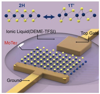
Schematic shows the configuration for structural phase transition on a molybdenum ditelluride monolayer (MoTe2, shown as yellow and blue spheres), which is anchored by a metal electrodes (top gate and ground). The ionic liquid covering the monolayer and electrodes enables a high density of electrons to populate the monolayer, leading to changes in the structural lattice from a hexagonal (2H) to monoclinic (1T’) pattern. (Credit: Ying Wang/Berkeley Lab)
In a study published today in the journal Nature, scientists have found a way to reversibly change the atomic structure of a 2-D material by injecting, or “doping,” it with electrons. The process uses far less energy than current methods for changing the configuration of a material’s structure.
“We show, for the first time, that it is possible to inject electrons to drive structural phase changes in materials,” said study principal investigator Xiang Zhang, senior faculty scientist at Berkeley Lab’s Materials Sciences Division and a professor at UC Berkeley. “By adding electrons into a material, the overall energy goes up and will tip off the balance, resulting in the atomic structure rearranging to a new pattern that is more stable. Such electron doping-driven structural phase transitions at the 2-D limit is not only important in fundamental physics; it also opens the door for new electronic memory and low-power switching in the next generation of ultra-thin devices.”
Switching a material’s structural configuration from one phase to another is the fundamental, binary characteristic that underlies today’s digital circuitry. Electronic components capable of this phase transition have shrunk down to paper-thin sizes, but they are still considered to be bulk, 3-D layers by scientists. By comparison, 2-D monolayer materials are composed of a single layer of atoms or molecules whose thickness is 100,000 times as small as a human hair.
“The idea of electron doping to alter a material’s atomic structure is unique to 2-D materials, which are much more electrically tunable compared with 3-D bulk materials,” said study co-lead author Jun Xiao, a graduate student in Zhang’s lab.
The classic approach to driving the structural transition of materials involves heating to above 500 degrees Celsius. Such methods are energy-intensive and not feasible for practical applications. In addition, the excess heat can significantly reduce the life span of components in integrated circuits.
A number of research groups have also investigated the use of chemicals to alter the configuration of atoms in semiconductor materials, but that process is still difficult to control and has not been widely adopted by industry.
“Here we use electrostatic doping to control the atomic configuration of a two-dimensional material,” said study co-lead author Ying Wang, another graduate student in Zhang’s lab. “Compared to the use of chemicals, our method is reversible and free of impurities. It has greater potential for integration into the manufacturing of cell phones, computers, and other electronic devices.”
The researchers used molybdenum ditelluride (MoTe2), a typical 2-D semiconductor, and coated it with an ionic liquid (DEME-TFSI), which has an ultra-high capacitance, or ability to store electric charges. The layer of ionic liquid allowed the researchers to inject the semiconductor with electrons at a density of a hundred trillion to a quadrillion per square centimeter. It is an electron density that is one to two orders higher in magnitude than what could be achieved in 3-D bulk materials, the researchers said.
Through spectroscopic analysis, the researchers determined that the injection of electrons changed the atoms’ arrangement of the molybdenum ditelluride from a hexagonal shape to one that is monoclinic, which has more of a slanted cuboid shape. Once the electrons were retracted, the crystal structure returned to its original hexagonal pattern, showing that the phase transition is reversible. Moreover, these two types of atom arrangements have very different symmetries, providing a large contrast for applications in optical components.
“Such an atomically thin device could have dual functions, serving simultaneously as optical or electrical transistors, and hence broaden the functionalities of the electronics used in our daily lives,” said Wang.
About Lawrence Berkeley National Laboratory
Lawrence Berkeley National Laboratory addresses the world’s most urgent scientific challenges by advancing sustainable energy, protecting human health, creating new materials, and revealing the origin and fate of the universe. Founded in 1931, Berkeley Lab’s scientific expertise has been recognized with 13 Nobel Prizes. The University of California manages Berkeley Lab for the U.S. Department of Energy’s Office of Science.
Share on:


Suggested Items
Real Time with... IPC APEX EXPO 2024: Sustainability in the Industry
04/26/2024 | Real Time with...IPC APEX EXPOGuest Editor Henry Crandall and Chris Nash of Indium Corporation discuss the company's 90th anniversary and its focus on sustainability. They focus on the benefits of sustainable materials, their compatibility, and value propositions. The conversation also highlights how Durafuse LT technology's role in reducing reflow temperatures is leading to significant cost and energy savings. Nash also touches on downstream sustainability efforts such as using recycled materials for packaging.
SMC Korea 2024 to Highlight Semiconductor Materials Trends and Innovations on Industry’s Path to $1 Trillion
04/24/2024 | SEMIWith Korea a major consumer of semiconductor materials and advanced materials a key driver of innovation on the industry’s path to $1 trillion, industry leaders and experts will gather at SMC (Strategic Materials Conference) Korea 2024 on May 29 at the Suwon Convention Center in Gyeonggi-do, South Korea to provide insights into the latest materials developments and trends. Registration is open.
Groundbreaking Ceremony Marks the Beginning of a New Era for Newccess Industrial; The Construction of the MINGXIN Building
04/12/2024 | Newccess IndustrialOn a clear and sunny day in March, the groundbreaking ceremony for the MINGXIN Building took place in Shenzhen, China. This moment marked the official commencement of construction for a project that will reshape the semiconductor materials industry.
The Need for a Holistic Global Sustainability Standard
04/10/2024 | Michael Ford, Aegis SoftwareNo one can deny that the resources of our fragile planet are finite. The environment seems like a third party, subject to constant degradation. We’re acutely aware of the effects of pollution on our climate, and despite our “throw-away” culture, recycling and recovery of materials has remained relatively expensive, even as we use more energy just to survive.
iNEMI Publishes Four Roadmap Topics
04/04/2024 | iNEMIThe International Electronics Manufacturing Initiative (iNEMI) announces the availability of the first roadmap topics in the new iNEMI Roadmap format. Printed circuit boards, sustainable electronics, smart manufacturing, and mmWave materials and test are now available online.