


 The Right Approach: I Hear the Train A Comin'
 It’s Only Common Sense: OCCAM—the Time Is Now
 Marcy's Musings: The Growing Industry
Additive Manufacturing May Hold Key to Transforming Nanomaterials Into Multifunctional Devices
November 7, 2017 | Notre DameEstimated reading time: 1 minute
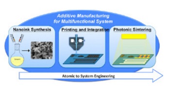
Nanomaterials have been widely studied and proven to have unique properties that make them more suited to a variety of applications. However, there is still a need to better understand their structure and property evolutions from nanoscale to macroscale as well as transform nanoscale materials into functional devices using scalable and low-cost manufacturing processes Yanliang Zhang, assistant professor of aerospace and mechanical engineering and participating faculty member in the Center for Nano Science and Technology and the Center for Sustainable Energy at the University of Notre Dame, is working to do both. He and his team in the Advanced Manufacturing and Energy Lab are developing an innovative and highly scalable additive manufacturing process that may hold the key to transform the nanomaterials into multifunctional devices. Their work aims to fabricate high-performance and flexible energy harvesters, sensors and electronic devices, an area that is undergoing tremendous growth.
Zhang and his team are focusing their efforts on two projects in particular, one funded through a National Science Foundation (NSF) CAREER Development Award and one funded through the U.S. Department of Energy (DOE) — both targeting additive manufacturing to convert colloidal nanocrystals into functional devices of unprecedented performances.
Through the NSF project, they will be studying the additive printing and sintering processes of colloidal nanocrystals to control thermoelectric and electronic properties in printed structures. They are working to establish a scalable and cost-effective additive manufacturing process to fabricate flexible thermoelectric and electronic films. These films offer a range of applications from energy harvesting and cooling to flexible electronics and devices. The fundamental research outcomes they develop will not only significantly advance the manufacturing processes for flexible thermoelectric and electronic materials but also generate new knowledge of processing-structure-property relationships in the additive printing of a variety of functional colloidal nanocrystals.
Zhang’s team is also developing advanced 3D conformal sensors using additive manufacturing through a DOE project. The goal of the project is to develop an additive manufacturing approach to directly print sensors onto nuclear fuel components and measure the thermal conductivity. Thermal conductivity is one of the most important nuclear fuel properties driving the heat transfer performance. Printing the sensors directly onto components enables high measurement accuracy with minimal intrusion. This research has the potential to establish a new sensor manufacturing paradigm for a broad range of industrial applications.
Share on:


Suggested Items
Real Time with… IPC APEX EXPO 2024: Tools, Training, and Trends in Manufacturing Engineering
04/25/2024 | Real Time with...IPC APEX EXPOGuest Editor Kelly Dack and Product Specialist Erik Bateham of Polar Instruments discuss Polar's latest technology, including their role in aiding manufacturing engineers. They highlight the advanced capabilities of Polar's tools and the critical role of signal integrity analysis, as well as the importance of accurate modeling in board manufacturing. Polar's unique training approach and demonstration contact details are also explored.
TTM Celebrates the Grand Opening of Its First Manufacturing Facility in Penang
04/25/2024 | TTM Technologies, Inc.TTM Technologies, Inc., a leading global manufacturer of technology solutions including mission systems, radio frequency (RF) components and RF microwave/microelectronic assemblies, and quick-turn and technologically advanced printed circuit boards (PCBs), officially opened its first manufacturing plant in Penang, Malaysia with an investment of USD200 million (approximately RM958 million).
Listen Up! The Intricacies of PCB Drilling Detailed in New Podcast Episode
04/25/2024 | I-Connect007In episode 5 of the podcast series, On the Line With: Designing for Reality, Nolan Johnson and Matt Stevenson continue down the manufacturing process, this time focusing on the post-lamination drilling process for PCBs. Matt and Nolan delve into the intricacies of the PCB drilling process, highlighting the importance of hole quality, drill parameters, and design optimization to ensure smooth manufacturing. The conversation covers topics such as drill bit sizes, aspect ratios, vias, challenges in drilling, and ways to enhance efficiency in the drilling department.
Elevating PCB Design Engineering With IPC Programs
04/24/2024 | Cory Blaylock, IPCIn a monumental stride for the electronics manufacturing industry, IPC has successfully championed the recognition of the PCB Design Engineer as an official occupation by the U.S. Department of Labor (DOL). This pivotal achievement not only underscores the critical role of PCB design engineers within the technology landscape, but also marks the beginning of a transformative journey toward nurturing a robust, skilled workforce ready to propel our industry into the future.
Fujitsu, METRON Collaborate to Drive ESG Success
04/24/2024 | JCN NewswireFujitsu Limited and METRON SAS, a French cleantech company specializing in energy management solutions for industrial decarbonization, today announced a strategic initiative to contribute to the realization of carbon neutrality in the manufacturing industry.