


 The Right Approach: I Hear the Train A Comin'
 It’s Only Common Sense: OCCAM—the Time Is Now
 Marcy's Musings: The Growing Industry
Watching Atoms Move in Hybrid Perovskite Crystals Reveals Clues to Improving Solar Cells
November 27, 2017 | UC San DiegoEstimated reading time: 2 minutes
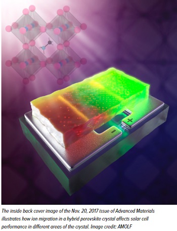
A team of researchers led by the University of California San Diego has for the first time observed nanoscale changes deep inside hybrid perovskite crystals that could offer new insights into developing low-cost, high-efficiency solar cells.
Using X-ray beams and lasers, researchers studied how a new promising class of solar cell materials, called hybrid perovskites, behaves at the nanoscale level during operation. Their experiments revealed that when voltage is applied, ions migrate within the material, creating regions that are no longer as efficient at converting light to electricity.
“Ion migration hurts the performance of the light absorbing material. Limiting it could be a key to improving the quality of these solar cells,” said David Fenning, a professor of nanoengineering and member of the Sustainable Power and Energy Center at UC San Diego.
The team, led by Fenning, includes researchers from the AMOLF Institute in the Netherlands and Argonne National Laboratory. Researchers published their findings in Advanced Materials.
Hybrid perovskites are crystalline materials made of a mixture of both inorganic and organic ions. They are promising materials for making next-generation solar cells because they are inexpensive to manufacture and are considerably efficient at converting light to electricity.
However, hybrid perovskites are not very stable, which can make them difficult to study. Microscopic techniques typically used to study solar cells often end up damaging the hybrid perovskites or can’t image beyond their surfaces.
Now, a UC San Diego-led team has shown that by using a technique called nanoprobe X-ray fluorescence, they can probe deep into hybrid perovskite materials without destroying them. “This is a new window to peer inside these materials and see precisely what’s going wrong,” Fenning said.
The researchers studied a type of hybrid perovskite called methylammonium lead bromide, which contains negatively charged bromine ions. Like other hybrid perovskites, its crystalline structure contains many vacancies, or missing atoms, which have been suspected to allow ions to move readily within the material when a voltage is applied.
The researchers first performed nanoprobe X-ray fluorescence measurements on the crystals to create high-resolution maps of the atoms inside the material. The maps revealed that when voltage is applied, the bromine ions migrate from negatively charged areas to positively charged areas.
Next, the researchers shined a laser on the crystals to measure a property called photoluminescence—the material’s ability to emit light when excited by a laser—in different areas of the crystals. A good solar cell material emits light very well, so the higher the photoluminescence, the more efficient the solar cell should be. The areas with higher bromine concentrations had up to 180 percent higher photoluminescence than areas depleted of bromine ions.
“We watch the bromine ions migrate within minutes and see that the resulting bromine-rich areas have the potential to become better solar cells while the performance is degraded in bromine-poor areas,” Fenning said.
Fenning and his team are now exploring ways to limit bromine migration in methylammonium lead bromide and other hybrid perovskites. Researchers say that one potential option would be growing hybrid perovskite crystals in different conditions to minimize the number of vacancies and limit ion migration in the crystalline structure.
Share on:


Suggested Items
Real Time with... IPC APEX EXPO 2024: Sustainability in the Industry
04/26/2024 | Real Time with...IPC APEX EXPOGuest Editor Henry Crandall and Chris Nash of Indium Corporation discuss the company's 90th anniversary and its focus on sustainability. They focus on the benefits of sustainable materials, their compatibility, and value propositions. The conversation also highlights how Durafuse LT technology's role in reducing reflow temperatures is leading to significant cost and energy savings. Nash also touches on downstream sustainability efforts such as using recycled materials for packaging.
SMC Korea 2024 to Highlight Semiconductor Materials Trends and Innovations on Industry’s Path to $1 Trillion
04/24/2024 | SEMIWith Korea a major consumer of semiconductor materials and advanced materials a key driver of innovation on the industry’s path to $1 trillion, industry leaders and experts will gather at SMC (Strategic Materials Conference) Korea 2024 on May 29 at the Suwon Convention Center in Gyeonggi-do, South Korea to provide insights into the latest materials developments and trends. Registration is open.
Groundbreaking Ceremony Marks the Beginning of a New Era for Newccess Industrial; The Construction of the MINGXIN Building
04/12/2024 | Newccess IndustrialOn a clear and sunny day in March, the groundbreaking ceremony for the MINGXIN Building took place in Shenzhen, China. This moment marked the official commencement of construction for a project that will reshape the semiconductor materials industry.
The Need for a Holistic Global Sustainability Standard
04/10/2024 | Michael Ford, Aegis SoftwareNo one can deny that the resources of our fragile planet are finite. The environment seems like a third party, subject to constant degradation. We’re acutely aware of the effects of pollution on our climate, and despite our “throw-away” culture, recycling and recovery of materials has remained relatively expensive, even as we use more energy just to survive.
iNEMI Publishes Four Roadmap Topics
04/04/2024 | iNEMIThe International Electronics Manufacturing Initiative (iNEMI) announces the availability of the first roadmap topics in the new iNEMI Roadmap format. Printed circuit boards, sustainable electronics, smart manufacturing, and mmWave materials and test are now available online.