


 The Right Approach: I Hear the Train A Comin'
 It’s Only Common Sense: OCCAM—the Time Is Now
 Marcy's Musings: The Growing Industry
Engineering Electron Pathways in 2D-Topological Insulators
December 4, 2017 | CIC nanoGUNEEstimated reading time: 2 minutes
In a recent article published in Physical Review Letters researchers from CIC nanoGUNE, the Rudolf Peierls Centre for Theoretical Physics of Oxford, together with colleagues from Wuerzburg and Stanford University reported new insight into the electronic conduction and interference on 2D-topological insulators - an exotic kind of insulators that conduct only at the edge and that could be key for the development of a new generation of electronic devices.
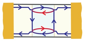
Image caption: Schematic representation of the electronic behavior in the device described in the article. The arrows represent quantum channels where electrons propagate. Eectrons are allowed to change direction only at the central area, resulting under certain conditions in constructive interference.Schematic representation of the electronic behavior in the device described in the article. The arrows represent quantum channels where electrons propagate. Eectrons are allowed to change direction only at the central area, resulting under certain conditions in constructive interference.
For decades, insulating materials were thought to be “boring” materials from an electronics point of view, since electrons are immobile and cannot contribute to electrical conduction. Recently, a different class of insulators was proposed and experimentally found. We call them “topological insulators”, as their electronic structure can be mathematically classified to be different than the usual, boring, “trivial” insulators.
A fascinating property of topological insulators is that while remaining insulating in the bulk, they are very good conductors at the edge. At those edges, electrons travel in quantum channels in either direction, like in a two- lane highway. Also like on a highway, U-turns are forbidden: electrons on the edge cannot change direction without breaking the rules. The application of an external magnetic field lifts this prohibition and allows electrons to turn.
The recently published research, lead by Reyes Calvo, Ikerbasque Fellow at CIC nanoGUNE, and Fernando de Juan, currently at Rudolf Peierls Centre for Theoretical Physics, Oxford and joining the Donostia International Phisics Centre (DIPC) as Ikerbasque Fellow in 2018, reports the interplay of quantum edge states across a lateral junction in a HgTe quantum well, a canonical 2D topological insulator. From their results, they extract new information on the fundamental properties of topological edge states and propose strategies to fine-tune their interaction.
"In our work, we test the consequences that allowing electrons to turn have in the conduction of our devices. We also show how under certain circumstances, electrons allowed to return seem to do it in an orderly manner, as if in some kind of round-about, generating a constructive interference.", Calvo explains.
This work contributes new insight into the fundamental properties of the edge states and their conduction properties in 2D-topological insulators. This kind of proposals to control the properties and interactions of these states are key for their application in the development of a new generation of electronic devices based on quantum fundamental properties of materials.
Share on:


Suggested Items
Book Excerpt: The Printed Circuit Assembler’s Guide to... Factory Analytics
04/24/2024 | I-Connect007 Editorial TeamIn our fast-changing, deeply competitive, and margin-tight industry, factory analytics can be the key to unlocking untapped improvements to guarantee a thriving business. On top of that, electronics manufacturers are facing a tremendous burden to do more with less. If you don't already have a copy of this book, what follows is an excerpt from the introduction chapter of 'The Printed Circuit Assembler’s Guide to... Factory Analytics: Unlocking Efficiency Through Data Insights' to whet your appetite.
Listen Up! The Intricacies of PCB Drilling Detailed in New Podcast Episode
04/25/2024 | I-Connect007In episode 5 of the podcast series, On the Line With: Designing for Reality, Nolan Johnson and Matt Stevenson continue down the manufacturing process, this time focusing on the post-lamination drilling process for PCBs. Matt and Nolan delve into the intricacies of the PCB drilling process, highlighting the importance of hole quality, drill parameters, and design optimization to ensure smooth manufacturing. The conversation covers topics such as drill bit sizes, aspect ratios, vias, challenges in drilling, and ways to enhance efficiency in the drilling department.
Elevating PCB Design Engineering With IPC Programs
04/24/2024 | Cory Blaylock, IPCIn a monumental stride for the electronics manufacturing industry, IPC has successfully championed the recognition of the PCB Design Engineer as an official occupation by the U.S. Department of Labor (DOL). This pivotal achievement not only underscores the critical role of PCB design engineers within the technology landscape, but also marks the beginning of a transformative journey toward nurturing a robust, skilled workforce ready to propel our industry into the future.
Winner of The Science Show Rakett 69 Receives Incap Scholarship
04/24/2024 | IncapThe winner of the Rakett 69 science show, Andri Türkson, who stood out as an electronics enthusiast, received a scholarship from Incap Estonia, along with an internship opportunity in Saaremaa.
Alternative Manufacturing Inc. Awarded QML Requalification to IPC J-STD-001 and IPC-A-610
04/24/2024 | IPCIPC's Validation Services Program has awarded an IPC J-STD-001 and IPC-A-610 Qualified Manufacturers Listing (QML) requalification to Alternative Manufacturing Inc (AMI).