


 The Right Approach: I Hear the Train A Comin'
 It’s Only Common Sense: OCCAM—the Time Is Now
 Marcy's Musings: The Growing Industry
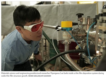
Beyond Silicon: Researchers Solve a Materials Mystery Key to Next-Generation Electronic Devices
February 6, 2018 | University of Wisconsin-MadisonEstimated reading time: 2 minutes
Lennon and McCartney. Abbott and Costello. Peanut butter and jelly.
Think of one half of any famous duo, and the other half likely comes to mind. Not only do they complement each other, but together they work better.
The same is true in the burgeoning field of oxide electronics materials. Boasting a wide array of behaviors, including electronic, magnetic and superconducting, these multifunctional materials are poised to expand the way we think about the functions of traditional silicon-based electronic devices such as cell phones or computers.
Yet until now, a critical aspect has been missing — one that complements the function of electrons in oxide electronics. And a team led by University of Wisconsin–Madison materials scientist Chang-Beom Eom has directly observed that missing second half of the duo necessary to move oxide electronics materials forward.
It’s called a two-dimensional hole gas — a counterpart to something known as a two-dimensional electron gas. For more than a decade, researchers have recognized a hole gas appearance was possible, but haven’t been able to create it experimentally.
“The 2D hole gas was not possible primarily because perfect-enough crystals could not be grown,” says Eom, the Theodore H. Geballe Professor and Harvey D. Spangler Distinguished Professor of materials science and engineering. “Inside, there were defects that killed the hole gas.”
Eom is a world expert in material growth, using techniques that allow him to meticulously build, or “grow,” each layer of a material with atomic precision. That expertise, combined with insight into the interaction between layers in their structure, was key in identifying the elusive 2D hole gas.
“We were able to design the correct structure and make near-perfect crystals, all without defects that degrade the hole gas,” he says.
Also important in identifying the hole gas was the almost-symmetrical way in which Eom assembled the various layers — something like a club sandwich. While other researchers have made the material in a bi-layer structure, Eom designed a triple layer. He alternated layers of strontium oxide and titanium dioxide on the bottom, then layers of lanthanum oxide and aluminum oxide, then added additional layers of strontium oxide and titanium dioxide on the top.
As a result, the hole gas forms at the interface of the layers on the top, while the electron gas forms at the interface of the layers on the bottom — the first demonstration of a very powerful complementary pair.
Just as people 50 years ago likely could not have envisioned communicating via wireless devices, the advance sets forth a platform that can enable new concepts-applications that today remain beyond our wildest dreams.
“We’re not just improving the performance of devices,” says Eom. “So, not improving a cell phone, for example — but envisioning an entirely new device made possible by this advance. This is the beginning of an exciting new path.”
Eom’s collaborators from UW–Madison include physics professor Mark Rzchowski and graduate students in materials science and engineering and physics, as well as collaborators from The Ohio State University, the University of Nebraska at Lincoln, Argonne National Laboratory, and Sungkyunkwan University and Pohang University of Science and Technology in Korea.
Share on:


Suggested Items
Warm Windows and Streamlined Skin Patches – IDTechEx Explores Flexible and Printed Electronics
04/26/2024 | IDTechExFlexible and printed electronics can be integrated into cars and homes to create modern aesthetics that are beneficial and easy to use. From luminous car controls to food labels that communicate the quality of food, the uses of this technology are endless and can upgrade many areas of everyday life.
Book Excerpt: The Printed Circuit Assembler’s Guide to... Factory Analytics
04/24/2024 | I-Connect007 Editorial TeamIn our fast-changing, deeply competitive, and margin-tight industry, factory analytics can be the key to unlocking untapped improvements to guarantee a thriving business. On top of that, electronics manufacturers are facing a tremendous burden to do more with less. If you don't already have a copy of this book, what follows is an excerpt from the introduction chapter of 'The Printed Circuit Assembler’s Guide to... Factory Analytics: Unlocking Efficiency Through Data Insights' to whet your appetite.
Listen Up! The Intricacies of PCB Drilling Detailed in New Podcast Episode
04/25/2024 | I-Connect007In episode 5 of the podcast series, On the Line With: Designing for Reality, Nolan Johnson and Matt Stevenson continue down the manufacturing process, this time focusing on the post-lamination drilling process for PCBs. Matt and Nolan delve into the intricacies of the PCB drilling process, highlighting the importance of hole quality, drill parameters, and design optimization to ensure smooth manufacturing. The conversation covers topics such as drill bit sizes, aspect ratios, vias, challenges in drilling, and ways to enhance efficiency in the drilling department.
Elevating PCB Design Engineering With IPC Programs
04/24/2024 | Cory Blaylock, IPCIn a monumental stride for the electronics manufacturing industry, IPC has successfully championed the recognition of the PCB Design Engineer as an official occupation by the U.S. Department of Labor (DOL). This pivotal achievement not only underscores the critical role of PCB design engineers within the technology landscape, but also marks the beginning of a transformative journey toward nurturing a robust, skilled workforce ready to propel our industry into the future.
Winner of The Science Show Rakett 69 Receives Incap Scholarship
04/24/2024 | IncapThe winner of the Rakett 69 science show, Andri Türkson, who stood out as an electronics enthusiast, received a scholarship from Incap Estonia, along with an internship opportunity in Saaremaa.