


 It’s Only Common Sense: Nice Guys Really Can Finish First
 The Right Approach: I Hear the Train A Comin'
 Marcy's Musings: The Growing Industry
MEMS Chips Get Metalenses
February 21, 2018 | AMERICAN INSTITUTE OF PHYSICSEstimated reading time: 2 minutes
Lens technologies have advanced across all scales, from digital cameras and high bandwidth in fiber optics to the LIGO lab instruments. Now, a new lens technology that could be produced using standard computer-chip technology is emerging and could replace the bulky layers and complex geometries of traditional curved lenses.
Flat lenses, unlike their traditional counterparts, are relatively lightweight, based on optical nanomaterials known as metasurfaces. When the subwavelength nanostructures of a metasurface form certain repeated patterns, they mimic the complex curvatures that refract light, but with less bulk and an improved ability to focus light with reduced distortion. However, most of these nanostructured devices are static, which limits their functionality.
Federico Capasso, an applied physicist at Harvard University who pioneered metalens technology, and Daniel Lopez, group leader of nanofabrication and devices at Argonne National Laboratory and an early developer of microelectromechanical systems (MEMS), brainstormed about adding motion capabilities like fast scanning and beam steering to metalenses for new applications.
Capasso and Lopez developed a device that integrates mid-infrared spectrum metalenses onto MEMS. The researchers report their findings this week in APL Photonics, from AIP Publishing.
MEMS is a circuit-based technology that incorporates microelectronics, like those found in computer chips, and includes mechanical microstructures like actuators and gears. Ubiquitous in everything from cellphones to airbags, biosensing devices, appliances and optics, MEMS are fabricated using the same techniques used for integrated circuits on typical computer chips.
"Dense integration of thousands of individually controlled lens-on-MEMS devices onto a single silicon chip would allow an unprecedented degree of control and manipulation of the optical field," Lopez Said.
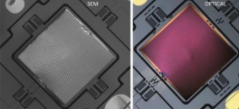
The researchers formed the metasurface lens using standard photolithography techniques on a silicon-on-insulator wafer with a 2-micron-thick top device layer, a 200-nanometer buried-oxide layer, and a 600-micron-thick handle layer. Then, they placed the flat lens onto a MEMS scanner, essentially a micromirror that deflects light for high-speed optical path length modulation. They aligned the lens with the MEMS' central platform and fixed them together by depositing small platinum patches.
"Our MEMS-integrated metasurface lens prototype can be electrically controlled to vary the angular rotation of a flat lens and can scan the focal spot by several degrees," Lopez said. "Furthermore, this proof-of-concept integration of metasurface-based flat lenses with MEMS scanners can be extended to the visible and other parts of the electromagnetic spectrum, implying the potential for application across wider fields, such as MEMS-based microscope systems, holographic and projection imaging, LIDAR (light detection and ranging) scanners and laser printing."
When electrostatically actuated, the MEMS platform controls the angle of the lens along two orthogonal axes, allowing the scanning of the flat lens focal spot by about 9 degrees in each direction. The researchers estimate that the focusing efficiency is about 85 percent.
"Such metalenses can be mass produced with the same computer-chip fabrication technology and in the future, will replace conventional lenses in a wide range of applications," Capasso said.
Share on:


Suggested Items
NextFlex Convenes the Hybrid Electronics Community at Binghamton University
05/01/2024 | NextFlexBinghamton University hosted the NextFlex hybrid electronics community on April 18 for a day of expert presentations, breakout sessions on technology and manufacturing topics, and networking.
IDTechEx Report on Quantum Technology: Nano-scale Physics for Massive Market Impact
04/30/2024 | PRNewswireThe quantum technology market leverages nano-scale physics to create revolutionary new devices for computing, sensing, and communications. Across the industry, quantum technology offers a paradigm shift in performance compared with incumbent solutions.
TSMC Certifies Ansys Multiphysics Platforms, Enabling Next-Gen AI and HPC Chips
04/30/2024 | PRNewswireAnsys announced the certification of its power integrity platforms for TSMC's N2 technology full production release. Both Ansys RedHawk-SC and Ansys Totem are certified for power integrity signoff on the N2 process, delivering significant speed and power advantages for high performance computing, mobile chips, and 3D-IC designs.
Koh Young Extends Invitation to the 2024 IEEE Electronic Components and Technology Conference
04/30/2024 | Koh YoungKoh Young, the industry leader in True3D measurement-based inspection solutions, invites you to join us at the at the 2024 IEEE Electronic Components and Technology Conference from May 28-31, 2024, in Denver, Colorado at the Gaylord Rockies Resort & Convention Center.
Samsung Electronics Begins Industry’s First Mass Production of 9th-Gen V-NAND
04/29/2024 | Samsung ElectronicsSamsung Electronics, the world leader in advanced memory technology, today announced that it has begun mass production for its one-terabit (Tb) triple-level cell (TLC) 9th-generation vertical NAND (V-NAND), solidifying its leadership in the NAND flash market.