


 It’s Only Common Sense: Create Passion That Customers Feel
 Punching Out: How to Stay Focused in Business and M&A


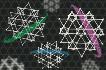
A motif of Japanese basketweaving known as the kagome pattern has preoccupied physicists for decades. Kagome baskets are typically made from strips of bamboo woven into a highly symmetrical pattern of interlaced, corner-sharing triangles.
If a metal or other conductive material could be made to resemble such a kagome pattern at the atomic scale, with individual atoms arranged in similar triangular patterns, it should in theory exhibit exotic electronic properties.
In a paper published today in Nature, physicists from MIT, Harvard University, and Lawrence Berkeley National Laboratory report that they have for the first time produced a kagome metal — an electrically conducting crystal, made from layers of iron and tin atoms, with each atomic layer arranged in the repeating pattern of a kagome lattice.
When they flowed a current across the kagome layers within the crystal, the researchers observed that the triangular arrangement of atoms induced strange, quantum-like behaviors in the passing current. Instead of flowing straight through the lattice, electrons instead veered, or bent back within the lattice.
This behavior is a three-dimensional cousin of the so-called Quantum Hall effect, in which electrons flowing through a two-dimensional material will exhibit a “chiral, topological state,” in which they bend into tight, circular paths and flow along edges without losing energy.
“By constructing the kagome network of iron, which is inherently magnetic, this exotic behavior persists to room temperature and higher,” says Joseph Checkelsky, assistant professor of physics at MIT. “The charges in the crystal feel not only the magnetic fields from these atoms, but also a purely quantum-mechanical magnetic force from the lattice. This could lead to perfect conduction, akin to superconductivity, in future generations of materials.”
To explore these findings, the team measured the energy spectrum within the crystal, using a modern version of an effect first discovered by Heinrich Hertz and explained by Einstein, known as the photoelectric effect.
“Fundamentally, the electrons are first ejected from the material’s surface and are then detected as a function of takeoff angle and kinetic energy,” says Riccardo Comin, an assistant professor of physics at MIT. “The resulting images are a very direct snapshot of the electronic levels occupied by electrons, and in this case they revealed the creation of nearly massless ‘Dirac’ particles, an electrically charged version of photons, the quanta of light.”
The spectra revealed that electrons flow through the crystal in a way that suggests the originally massless electrons gained a relativistic mass, similar to particles known as massive Dirac fermions. Theoretically, this is explained by the presence of the lattice’s constituent iron and tin atoms. The former are magnetic and give rise to a “handedness,” or chirality. The latter possess a heavier nuclear charge, producing a large local electric field. As an external current flows by, it senses the tin’s field not as an electric field but as a magnetic one, and bends away.
The research team was led by Checkelsky and Comin, as well as graduate students Linda Ye and Min Gu Kang in collaboration with Liang Fu, the Biedenharn Associate Professor of Physics, and postdoc Junwei Liu. The team also includes Christina Wicker ’17, research scientist Takehito Suzuki of MIT, Felix von Cube and David Bell of Harvard, and Chris Jozwiak, Aaron Bostwick, and Eli Rotenberg of Lawrence Berkeley National Laboratory.
“No alchemy required”
Physicists have theorized for decades that electronic materials could support exotic Quantum Hall behavior with their inherent magnetic character and lattice geometry. It wasn’t until several years ago that researchers made progress in realizing such materials.
“The community realized, why not make the system out of something magnetic, and then the system’s inherent magnetism could perhaps drive this behavior,” says Checkelsky, who at the time was working as a researcher at the University of Tokyo.
This eliminated the need for laboratory produced fields, typically 1 million times as strong as the Earth’s magnetic field, needed to observe this behavior.
“Several research groups were able to induce a Quantum Hall effect this way, but still at ultracold temperatures a few degrees above absolute zero — the result of shoehorning magnetism into a material where it did not naturally occur,” Checkelsky says.
At MIT, Checkelsky has instead looked for ways to drive this behavior with “instrinsic magnetism.” A key insight, motivated by the doctoral work of Evelyn Tang PhD ’15 and Professor Xiao-Gang Wen, was to seek this behavior in the kagome lattice. To do so, first author Ye ground together iron and tin, then heated the resulting powder in a furnace, producing crystals at about 750 degrees Celsius — the temperature at which iron and tin atoms prefer to arrange in a kagome-like pattern. She then submerged the crystals in an ice bath to enable the lattice patterns to remain stable at room temperature.
“The kagome pattern has big empty spaces that might be easy to weave by hand, but are often unstable in crystalline solids which prefer the best packing of atoms,” Ye says. “The trick here was to fill these voids with a second type of atom in a structure that was at least stable at high temperatures. Realizing these quantum materials doesn’t need alchemy, but instead materials science and patience.”
Page 1 of 2


