


 The Right Approach: I Hear the Train A Comin'
 It’s Only Common Sense: OCCAM—the Time Is Now
 Marcy's Musings: The Growing Industry
IHEP Develops First CMOS Pixel Sensor Prototype for Circular Electron Positron Collider
October 10, 2018 | Chinese Academy of SciencesEstimated reading time: 1 minute
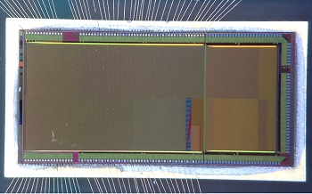
Scientists from the Institute of High Energy Physics (IHEP) have developed the first pixel sensor prototype based on the 180 nm Complementary Metal–Oxide–Semiconductor (CMOS) imaging sensor process recently. This represents significant progress in the key technology of the micro-vertex detector, the core component for the detector at the Circular Electron Positron Collider (CEPC).
CMOS pixel sensors allow integration of the sensing element and its readout electronics on the same silicon substrate, which make them attractive for charged particle tracking. The CEPC micro-vertex detector, located closest to the e+e- interaction point, will use state-of-the-art pixel technologies that provide high spatial resolution, are capable of high readout speed and adequate radiation hardness, and feature low power consumption.
The first prototype sensors, named JadePix 1, have been characterized with radioactive resources, and recently by the electron test beam at DESY in Hamburg, Germany. Preliminary results show that spatial resolutions better than 5 μm and 3.5 μm can be achieved for pixel sizes of 33×33 μm2 and 16×16 μm2, respectively. More importantly, there is no significant resolution degradation after exposure to neutron irradiation up to 1013 1 MeV neq/cm2.
The proposed Circular Electron Positron Collider (CEPC) aims at measuring Higgs properties with high precision and probing new physics beyond the Standard Model of particle physics. The CEPC Study Group has completed the conceptual design report (CDR) for the e+e- collider, and is completing the CDR for the detector. The group is pursuing an R&D program involving technologies critical for realizing the CEPC.
IHEP's Experimental Physics Division (EPD) initiated the R&D project to develop the novel CMOS pixel sensors. The advanced silicon tracking detectors and associated electronics have been the focal research direction at EPD. The division has been actively participating in several international projects, including the ATLAS Inner Tracker Upgrade, to gain design and construction experience for silicon detectors.
In addition, the division has developed pixel detectors for X-ray imaging. These detectors will soon be deployed at various stations of the High Energy Photon Source (HEPS), which will be constructed near Beijing. Meanwhile, EPD is pushing forward pixel detector R&D for the CEPC using both CMOS and SOI technologies. The goal is to design a fully functional pixel sensor and construct a larger scale prototype detector in near future.
Share on:


Suggested Items
iNEMI Packaging Tech Topic Series: Role of EDA in Advanced Semiconductor Packaging
04/26/2024 | iNEMIAdvanced semiconductor packaging with heterogenous integration has made on-package integration of multiple chips a crucial part of finding alternatives to transistor scaling. Historically, EDA tools for front-end and back-end design have evolved separately; however, design complexity and the increased number of die-to-die or die-to-substrate interconnections has led to the need for EDA tools that can support integration of overall design planning, implementation, and system analysis in a single cockpit.
Cadence, TSMC Collaborate on Wide-Ranging Innovations to Transform System and Semiconductor Design
04/25/2024 | Cadence Design SystemsCadence Design Systems, Inc. and TSMC have extended their longstanding collaboration by announcing a broad range of innovative technology advancements to accelerate design, including developments ranging from 3D-IC and advanced process nodes to design IP and photonics.
Ansys, TSMC Enable a Multiphysics Platform for Optics and Photonics, Addressing Needs of AI, HPC Silicon Systems
04/25/2024 | PRNewswireAnsys announced a collaboration with TSMC on multiphysics software for TSMC's Compact Universal Photonic Engines (COUPE). COUPE is a cutting-edge Silicon Photonics (SiPh) integration system and Co-Packaged Optics platform that mitigates coupling loss while significantly accelerating chip-to-chip and machine-to-machine communication.
Siemens’ Breakthrough Veloce CS Transforms Emulation and Prototyping with Three Novel Products
04/24/2024 | Siemens Digital Industries SoftwareSiemens Digital Industries Software launched the Veloce™ CS hardware-assisted verification and validation system. In a first for the EDA (Electronic Design Automation) industry, Veloce CS incorporates hardware emulation, enterprise prototyping and software prototyping and is built on two highly advanced integrated circuits (ICs) – Siemens’ new, purpose-built Crystal accelerator chip for emulation and the AMD Versal™ Premium VP1902 FPGA adaptive SoC (System-on-a-chip) for enterprise and software prototyping.
Listen Up! The Intricacies of PCB Drilling Detailed in New Podcast Episode
04/25/2024 | I-Connect007In episode 5 of the podcast series, On the Line With: Designing for Reality, Nolan Johnson and Matt Stevenson continue down the manufacturing process, this time focusing on the post-lamination drilling process for PCBs. Matt and Nolan delve into the intricacies of the PCB drilling process, highlighting the importance of hole quality, drill parameters, and design optimization to ensure smooth manufacturing. The conversation covers topics such as drill bit sizes, aspect ratios, vias, challenges in drilling, and ways to enhance efficiency in the drilling department.