


 The Right Approach: I Hear the Train A Comin'
 It’s Only Common Sense: OCCAM—the Time Is Now
 Marcy's Musings: The Growing Industry
NASA to Advance Unique 3D Printed Sensor Technology
February 18, 2019 | NASAEstimated reading time: 4 minutes
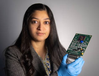
A NASA technologist is taking miniaturization to the extreme.
Mahmooda Sultana won funding to advance a potentially revolutionary, nanomaterial-based detector platform. The technology is capable of sensing everything from minute concentrations of gases and vapor, atmospheric pressure and temperature, and then transmitting that data via a wireless antenna — all from the same self-contained platform that measures just two-by-three-inches in size.
Image Caption: Technologist Mahmooda Sultana holds an early iteration of an autonomous multifunctional sensor platform, which could benefit all of NASA's major scientific disciplines and efforts to send humans to the Moon and Mars. Credits: NASA/W. Hrybyk
Under a $2 million technology development award, Sultana and her team at NASA’s Goddard Space Flight Center in Greenbelt, Maryland, will spend the next two years advancing the autonomous multifunctional sensor platform. If successful the technology could benefit NASA’s major science disciplines and efforts to send humans to the Moon and Mars. These tiny platforms could be deployed on planetary rovers to detect small quantities of water and methane, for example, or be used as monitoring or biological sensors to maintain astronaut health and safety.
Central to the effort, funded by NASA’s Space Technology Mission Directorate’s (STMD) Early Career Initiative (ECI) is a 3D printing system developed by Ahmed Busnina and his group at Northeastern University in Boston. The 3D printing system is like printers used to produce money or newspapers. However, instead of ink, the printer applies nanomaterials, layer-by-layer, onto a substrate to create tiny sensors. Ultimately, each is capable of detecting a different gas, pressure level or temperature.
Nanomaterials, such as carbon nanotubes, graphene, molybdenum disulfide and others, exhibit interesting physical properties. They are highly sensitive and stable at extreme conditions. They are also lightweight, hardened against radiation and require less power, making them ideal for space applications, Sultana said.
Under her partnership with Northeastern University, Sultana and her group will design the sensor platform, determining which combination of materials are best for measuring minute, parts-per-billion concentrations of water, ammonia, methane and hydrogen — all important in the search for life throughout the solar system. Using her design, Northeastern University will then use its Nanoscale Offset Printing System to apply the nanomaterials. Once printed, Sultana’s group will functionalize the individual sensors by depositing additional layers of nanoparticles to enhance their sensitivity, integrate the sensors with readout electronics, and package the entire platform.
The approach differs dramatically from how technologists currently fabricate multifunctional sensor platforms. Instead of building one sensor at a time and then integrating it to other components, 3D printing allows technicians to print a suite of sensors on one platform, dramatically simplifying the integration and packaging process.
Meet Mahmooda Sultana, Associate Branch Head, Systems Engineering Branch at NASA's Goddard Space Flight Center in Maryland. Mahmooda uses her love of math and puzzles to develop new technologies and miniaturize instruments for NASA missions.
Also innovative is Sultana’s plan to print on the same silicon wafer partial circuitry for a wireless communications system that would communicate with ground controllers, further simplifying instrument design and construction. Once printed, the sensors and wireless antenna will be packaged onto a printed circuit board that holds the electronics, a power source, and the rest of the communications circuitry.
“The beauty of our concept is that we’re able to print all sensors and partial circuity on the same substrate, which could be rigid or flexible. We eliminate a lot of the packaging and integration challenges,” Sultana said. “This is truly a multifunctional sensor platform. All my sensors are on same chip, printed one after another in layers.”
Wide-Ranging Uses
The research picks up where other NASA-funded efforts ended. Under several previous efforts funded by Goddard’s Internal Research and Development Program and STMD’s Center Innovation Fund, Sultana and her team used the same technique to manufacture and demonstrate individual sensors made of carbon nanotubes and molybdenum disulfide, among other materials. “The sensors were found to be quite sensitive, down to low parts per million. With our ECI funding, we are targeting the instrument’s sensitivity to parts per billion by improving sensor design and structure,” Sultana said.
According to her, the project addresses NASA’s need for low-power, small, lightweight, and highly sensitive sensors that can distinguish important molecules other than by measuring the masses of a molecule’s fragments, which is how many missions currently detect molecules today using mass spectrometers.
In fact, the agency has acknowledged that future sensors need to detect minute concentrations of gases and vapors in the parts per billion level. Although mass spectrometers can detect a wide spectrum of molecules — particularly useful for unknown samples — they have difficulty distinguishing between some of the important species, such as water, methane and ammonia. “It’s also difficult to reach the parts per billion or beyond level with them,” she said.
“We’re really excited about the possibilities of this technology,” Sultana said. “With our funding, we can take this technology to the next level and potentially offer NASA a new way to create customized, multifunctional sensor platforms, which I believe could open the door to all types of mission concepts and uses. The same approach we use to identify gases on a planetary body also could be used to create biological sensors that monitor astronaut health and the levels of contaminants inside spacecraft and living quarters.”
Share on:


Suggested Items
Koh Young Showcases Award-winning Inspection Solutions at SMTconnect with SmartRep in Hall 4A.225
04/25/2024 | Koh Young TechnologyKoh Young Technology, the industry leader in True 3D measurement-based inspection solutions, will showcase an array of award-winning inspection and measurement solutions at SMTconnect alongside its sales partner, SmartRep, in booth 4A.225 at NürnbergMesse from June 11-13, 2023. The following offers a glimpse into what Koh Young will present at the tradeshow:
Real Time with… IPC APEX EXPO 2024: Plasmatreat: Innovative Surface Preparation Solutions
04/25/2024 | Real Time with...IPC APEX EXPOIn this interview, Editor Nolan Johnson speaks with Hardev Grewal, CEO and president of Plasmatreat, a developer of atmospheric plasma solutions. Plasmatreat uses clean compressed air and electricity to create plasma, offering environmentally friendly methods for surface preparation. Their technology measures plasma density for process optimization and can remove organic micro-contamination. Nolan and Hardev also discuss REDOX-Tool, a new technology for removing metal oxides.
Nanotechnology Market to Surpass $53.51 Billion by 2031
04/25/2024 | PRNewswireSkyQuest projects that the nanotechnology market will attain a value of USD 53.51 billion by 2031, with a CAGR of 36.4% over the forecast period (2024-2031).
Cadence, TSMC Collaborate on Wide-Ranging Innovations to Transform System and Semiconductor Design
04/25/2024 | Cadence Design SystemsCadence Design Systems, Inc. and TSMC have extended their longstanding collaboration by announcing a broad range of innovative technology advancements to accelerate design, including developments ranging from 3D-IC and advanced process nodes to design IP and photonics.
SMC Korea 2024 to Highlight Semiconductor Materials Trends and Innovations on Industry’s Path to $1 Trillion
04/24/2024 | SEMIWith Korea a major consumer of semiconductor materials and advanced materials a key driver of innovation on the industry’s path to $1 trillion, industry leaders and experts will gather at SMC (Strategic Materials Conference) Korea 2024 on May 29 at the Suwon Convention Center in Gyeonggi-do, South Korea to provide insights into the latest materials developments and trends. Registration is open.