


 The Right Approach: I Hear the Train A Comin'
 It’s Only Common Sense: OCCAM—the Time Is Now
 Marcy's Musings: The Growing Industry
Electronic Chip Mimics the Brain to Make Memories in a Flash
July 16, 2019 | RMIT UniversityEstimated reading time: 2 minutes
Researchers from RMIT University drew inspiration from an emerging tool in biotechnology—optogenetics—to develop a device that replicates the way the brain stores and loses information.
Optogenetics allows scientists to delve into the body's electrical system with incredible precision, using light to manipulate neurons so that they can be turned on or off.
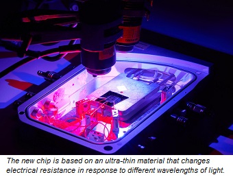
The new chip is based on an ultra-thin material that changes electrical resistance in response to different wavelengths of light, enabling it to mimic the way that neurons work to store and delete information in the brain.
Research team leader Dr Sumeet Walia said the technology moves us closer towards artificial intelligence (AI) that can harness the brain's full sophisticated functionality.
"Our optogenetically-inspired chip imitates the fundamental biology of nature's best computer - the human brain," Walia said. "Being able to store, delete and process information is critical for computing, and the brain does this extremely efficiently. "We're able to simulate the brain's neural approach simply by shining different colours onto our chip. "This technology takes us further on the path towards fast, efficient and secure light-based computing. "It also brings us an important step closer to the realisation of a bionic brain - a brain-on-a-chip that can learn from its environment just like humans do."
Dr Taimur Ahmed, lead author of the study published in Advanced Functional Materials, said being able to replicate neural behavior on an artificial chip offered exciting avenues for research across sectors.
"This technology creates tremendous opportunities for researchers to better understand the brain and how it's affected by disorders that disrupt neural connections, like Alzheimer's disease and dementia," Ahmed said.
The researchers, from the Functional Materials and Microsystems Research Group at RMIT, have also demonstrated the chip can perform logic operations—information processing—ticking another box for brain-like functionality.
Developed at RMIT's MicroNano Research Facility, the technology is compatible with existing electronics and has also been demonstrated on a flexible platform, for integration into wearable electronics.
How the chip works:
Neural connections happen in the brain through electrical impulses. When tiny energy spikes reach a certain threshold of voltage, the neurons bind together—and you've started creating a memory.
On the chip, light is used to generate a photocurrent. Switching between colors causes the current to reverse direction from positive to negative. This direction switch, or polarity shift, is equivalent to the binding and breaking of neural connections, a mechanism that enables neurons to connect (and induce learning) or inhibit (and induce forgetting). This is akin to optogenetics, where light-induced modification of neurons causes them to either turn on or off, enabling or inhibiting connections to the next neuron in the chain.
To develop the technology, the researchers used a material called black phosphorus (BP) that can be inherently defective in nature. This is usually a problem for optoelectronics, but with precision engineering the researchers were able to harness the defects to create new functionality.
"Defects are usually looked on as something to be avoided, but here we're using them to create something novel and useful," Ahmed said. "It's a creative approach to finding solutions for the technical challenges we face."
Share on:


Suggested Items
Warm Windows and Streamlined Skin Patches – IDTechEx Explores Flexible and Printed Electronics
04/26/2024 | IDTechExFlexible and printed electronics can be integrated into cars and homes to create modern aesthetics that are beneficial and easy to use. From luminous car controls to food labels that communicate the quality of food, the uses of this technology are endless and can upgrade many areas of everyday life.
iNEMI Packaging Tech Topic Series: Role of EDA in Advanced Semiconductor Packaging
04/26/2024 | iNEMIAdvanced semiconductor packaging with heterogenous integration has made on-package integration of multiple chips a crucial part of finding alternatives to transistor scaling. Historically, EDA tools for front-end and back-end design have evolved separately; however, design complexity and the increased number of die-to-die or die-to-substrate interconnections has led to the need for EDA tools that can support integration of overall design planning, implementation, and system analysis in a single cockpit.
Koh Young Showcases Award-winning Inspection Solutions at SMTconnect with SmartRep in Hall 4A.225
04/25/2024 | Koh Young TechnologyKoh Young Technology, the industry leader in True 3D measurement-based inspection solutions, will showcase an array of award-winning inspection and measurement solutions at SMTconnect alongside its sales partner, SmartRep, in booth 4A.225 at NürnbergMesse from June 11-13, 2023. The following offers a glimpse into what Koh Young will present at the tradeshow:
Real Time with… IPC APEX EXPO 2024: Plasmatreat: Innovative Surface Preparation Solutions
04/25/2024 | Real Time with...IPC APEX EXPOIn this interview, Editor Nolan Johnson speaks with Hardev Grewal, CEO and president of Plasmatreat, a developer of atmospheric plasma solutions. Plasmatreat uses clean compressed air and electricity to create plasma, offering environmentally friendly methods for surface preparation. Their technology measures plasma density for process optimization and can remove organic micro-contamination. Nolan and Hardev also discuss REDOX-Tool, a new technology for removing metal oxides.
Nanotechnology Market to Surpass $53.51 Billion by 2031
04/25/2024 | PRNewswireSkyQuest projects that the nanotechnology market will attain a value of USD 53.51 billion by 2031, with a CAGR of 36.4% over the forecast period (2024-2031).