


 The Right Approach: I Hear the Train A Comin'
 It’s Only Common Sense: OCCAM—the Time Is Now
 Marcy's Musings: The Growing Industry
Flexible and Stretchable Circuit Technologies for Space Applications
June 19, 2015 | M. Cauwe, F. Bossuyt, J. De Baets, and J. Vanfleteren, Laboratory for Advanced Research in Microelectronics (imec) Ghent UniversityEstimated reading time: 2 minutes
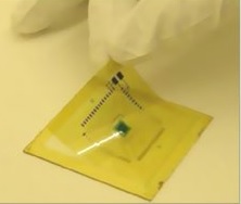
Flexible and stretchable circuit technologies offer reduced volume and weight, increased electrical performance, larger design freedom and improved interconnect reliability. All of these advantages are appealing for space applications. In this paper, two example technologies, the ultra-thin chip package (UTCP) and stretchable moulded interconnect (SMI), are described. The UTCP technology results in a 60μm thick chip package, including the embedding of a 20 μm thick chip, laser or protolithic via definition to the chip contacts and application of fan-out metallization. Imec’s stretchable interconnect technology is inspired by conventional rigid and flexible printed circuit board (PCB) technology. Stretchable interconnects are realized by copper meanders supported by a flexible material (e.g., polyimide). Elastic materials, predominantly silicone rubbers, are used to embed the conductors and the components, thus serving as circuit carrier. The possible advantages of these technologies with respect to space applications are discussed.
The driving application for flexible and stretchable circuit technologies is consumer electronics, especially handheld and mobile devices, which benefit the most from the reduction in form factor, the increased functional density and enlarged user comfort that is made possible with these technologies. Reduced volume and weight, increased electrical performance, larger design freedom and improved interconnect reliability are benefits that are also appealing for space applications.
Traditionally, electronics and sensor circuits are fabricated on flat rigid substrates, like FR-4 PCBs. In this conventional technology, packaged integrated circuits (ICs) and passive components are assembled onto the rigid PCB by soldering. For many applications, especially for mobile, portable, wearable and implantable electronics, the circuit should preferably be seamlessly integrated into the object that is used for transportation, is carried along, or worn on or inside the body. The electronics should be comfortable and unnoticeable to the user. In general, standard circuits do not fulfil these requirements. The user comfort can be increased in two ways. Extreme miniaturisation of the circuit reduces the presence of the system. A second approach is to transform the flat rigid circuit into a three-dimensional, conformable variant, following the random shape of the object or body part onto which it is integrated.
In this contribution, two original technologies developed at imec-CMST are presented. The ultra-thin chip package (UTCP) technology embeds 20–30 μm thick chips in a stack of spin-on polyimide (PI) layers. Adding thinfilm, fan-out metallization results in an extremely miniaturized, lightweight and flexible chip package with a total thickness below 100μm. Next to flexible electronics, a number of technologies for dynamically or one-time deformable stretchable circuits are under development. The stretchable concept is based on the interconnection of individual components or component islands with meander shaped metal wirings and embedding in elastic polymers like silicone rubbers (PDMS), polyurethanes (PU) or other plastics.
Editor's Note: This article originally appeared in the June 2015 issue of The PCB Magazine.
Share on:


Suggested Items
Warm Windows and Streamlined Skin Patches – IDTechEx Explores Flexible and Printed Electronics
04/26/2024 | IDTechExFlexible and printed electronics can be integrated into cars and homes to create modern aesthetics that are beneficial and easy to use. From luminous car controls to food labels that communicate the quality of food, the uses of this technology are endless and can upgrade many areas of everyday life.
Book Excerpt: The Printed Circuit Assembler’s Guide to... Factory Analytics
04/24/2024 | I-Connect007 Editorial TeamIn our fast-changing, deeply competitive, and margin-tight industry, factory analytics can be the key to unlocking untapped improvements to guarantee a thriving business. On top of that, electronics manufacturers are facing a tremendous burden to do more with less. If you don't already have a copy of this book, what follows is an excerpt from the introduction chapter of 'The Printed Circuit Assembler’s Guide to... Factory Analytics: Unlocking Efficiency Through Data Insights' to whet your appetite.
Listen Up! The Intricacies of PCB Drilling Detailed in New Podcast Episode
04/25/2024 | I-Connect007In episode 5 of the podcast series, On the Line With: Designing for Reality, Nolan Johnson and Matt Stevenson continue down the manufacturing process, this time focusing on the post-lamination drilling process for PCBs. Matt and Nolan delve into the intricacies of the PCB drilling process, highlighting the importance of hole quality, drill parameters, and design optimization to ensure smooth manufacturing. The conversation covers topics such as drill bit sizes, aspect ratios, vias, challenges in drilling, and ways to enhance efficiency in the drilling department.
Elevating PCB Design Engineering With IPC Programs
04/24/2024 | Cory Blaylock, IPCIn a monumental stride for the electronics manufacturing industry, IPC has successfully championed the recognition of the PCB Design Engineer as an official occupation by the U.S. Department of Labor (DOL). This pivotal achievement not only underscores the critical role of PCB design engineers within the technology landscape, but also marks the beginning of a transformative journey toward nurturing a robust, skilled workforce ready to propel our industry into the future.
Winner of The Science Show Rakett 69 Receives Incap Scholarship
04/24/2024 | IncapThe winner of the Rakett 69 science show, Andri Türkson, who stood out as an electronics enthusiast, received a scholarship from Incap Estonia, along with an internship opportunity in Saaremaa.