


 The Right Approach: I Hear the Train A Comin'
 It’s Only Common Sense: OCCAM—the Time Is Now
 Marcy's Musings: The Growing Industry
Silver: The Promising Electrode Winner for Low-Cost Perovskite Solar Cells
October 16, 2015 | OISTEstimated reading time: 3 minutes
Perovskite solar cells are the rising star in photovoltaics. They absorb light across almost all visible wavelengths, they have exceptional power conversion efficiencies exceeding 20% in the lab, and they are relatively easy to fabricate. So, why are perovskite solar cells yet to be found on the top of our roofs? One problem is their overall cost, and another is that cheaper perovskite solar cells have a short lifespan. A study published in Advanced Materials Interfaces by the Energy Materials and Surface Sciences Unit at the Okinawa Institute of Science and Technology Graduate University (OIST), reveals a cause for the short lifetime of perovskite solar cells with silver electrodes.
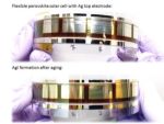
Currently, the most common electrode material in perovskite solar cells is gold, which is extremely expensive. A low-cost alternative to gold is silver, around 65 times cheaper. To keep the cost even lower, the team wants to use solution-processed method to fabricate the layers of the solar cell, instead of expensive vacuum-based techniques. The problem of using silver electrodes and the solution-based method is that silver gets corroded within days of the solar cell fabrication. The corrosion makes the electrode turn yellow, and reduces the efficiency of the cell. The OIST team, headed by Prof. Yabing Qi, has demonstrated the cause of this degradation and proposed an explanation.
Perovskite solar cells are composed of a sandwich of layers that work together to transform light into electricity. Light is absorbed by the perovskite material and stimulates electron excitations, generating the so-called electron-hole pairs. In simple terms: when electrons are excited, they “jump and leave holes behind.” Excited electrons and holes are transported in opposite directions by the adjacent layers of the solar cells, comprising of an electron-transport titanium dioxide layer, a spiro-MeOTAD hole-transport layer (HTL), a glass layer coated with a transparent conductive material, and a silver top electrode. The whole mechanism generates current, but it needs the correct functioning of each layer of the solar cell in order to work efficiently. “If one layer fails, the whole solar cell will suffer,” explains Luis Ono, a staff scientist and group leader in Prof. Qi’s unit.
In this study, the team analysed the composition of the corroded silver electrode and identified the formation of silver iodide as the reason for the electrode corrosion. The color change was due to the oxidation from silver to silver iodide. They also found that exposure to air accelerates the corrosion, when compared to dry nitrogen gas exposure.
The team proposed a mechanism for this damage: silver iodide forms because gas molecules from ambient air reach the perovskite material and degrade it forming iodine containing compounds. These iodine-containing compounds diffuse to the silver electrode and corrode it. The migration of both air molecules and iodine-containing compounds could happen through small pinholes present in the spiro-MeOTAD HTL layer (see animation). The pinholes present in the spiro-MeOTAD HTL layer produced with the solution-processed method were identified some months ago by Zafer Hawash, a PhD student in the same laboratory.
The animation shows the layers of the perovskite solar cell and the proposed mechanism of corrosion of the silver electrode. Water molecules diffuse through the pinholes of the spiro-MeOTAD layer and induce the decomposition of the perovskite producing iodine-containing compounds. The iodine-containing compounds migrate to the silver layer, and corrode it. This can explain why silver iodide is found on corroded solar cells. (Energy Materials and Surface Sciences Unit, OIST)
Replacing gold with silver and using the solution-processed method are key to bringing down the cost of the solar cells. The OIST team believes that understanding the corrosion mechanism is the first step in increasing the electrode lifetime. Since preventing the formation of pinholes in the spiro-MeOTAD HTL layer is essential for a longer cell lifetime, the team is also working on producing pinhole-free solar cells with the solution-process method, while the production of pinhole-free HTL with the vacuum-based method has already been published by the same group. “Perovskite-based solar cells show potential for commercial use as the next generation photovoltaic technology. Our goal is to design and fabricate large-area and low-cost photovoltaic modules with extended lifetime by employing appropriate HTLs and encapsulation materials,” explains Qi.
Share on:


Suggested Items
Designer’s Notebook: What Designers Need to Know About Manufacturing, Part 2
04/24/2024 | Vern Solberg -- Column: Designer's NotebookThe printed circuit board (PCB) is the primary base element for providing the interconnect platform for mounting and electrically joining electronic components. When assessing PCB design complexity, first consider the component area and board area ratio. If the surface area for the component interface is restricted, it may justify adopting multilayer or multilayer sequential buildup (SBU) PCB fabrication to enable a more efficient sub-surface circuit interconnect.
Happy’s Tech Talk #27: Integrated Mesh Power System (IMPS) for PCBs
04/08/2024 | Happy Holden -- Column: Happy’s Tech TalkA significant decrease in HDI substrate production cost can be achieved by reducing the number of substrate layers from conventional through-hole multilayers and microvia multilayers of eight, 10, 12, and more to only two layers. Besides reducing direct processing steps, the yield will increase as defect-producing operations are eliminated. The integrated mesh power system (IMPS) was invented in the latter years of MCM-D use for thin-film fabrication. Those geometries fit today into our use of ultra HDI.
Insulectro’s 'Storekeepers' Extend Their Welcome to Technology Village at IPC APEX EXPO
04/03/2024 | InsulectroInsulectro, the largest distributor of materials for use in the manufacture of PCBs and printed electronics, welcomes attendees to its TECHNOLOGY VILLAGE during this year’s IPC APEX EXPO at the Anaheim Convention Center, April 9-11, 2024.
Now Available: Episode 4, Season 2 of Designing for Reality—Lamination
04/04/2024 | I-Connect007I-Connect007 has just released the latest episode of its podcast series, On the Line With..., which focuses on designing for reality in the electronics industry. Multilayer boards bring along a completely different set of processes. In this installment, ASC Sunstone VP/Manager Matt Stevenson discusses manufacturing techniques for multilayer boards. Of course, this necessitates a review of drill and registration techniques, followed by the ins and outs of lamination.
Heavy Copper PCBs: Bridging the Gap Between Design and Fabrication, Part 1
04/01/2024 | Yash Sutariya, Saturn Electronics ServicesThey call me Sparky. This is due to my talent for getting shocked by a variety of voltages and because I cannot seem to keep my hands out of power control cabinets. While I do not have the time to throw the knife switch to the off position, that doesn’t stop me from sticking screwdrivers into the fuse boxes. In all honesty, I’m lucky to be alive. Fortunately, I also have a talent for building high-voltage heavy copper circuit boards. Since this is where I spend most of my time, I can guide you through some potential design for manufacturability (DFM) hazards you may encounter with heavy copper design.