


 The Right Approach: I Hear the Train A Comin'
 It’s Only Common Sense: OCCAM—the Time Is Now
 Marcy's Musings: The Growing Industry
Finessing Miniaturized Magnetics into the Microelectronics Mix
June 20, 2016 | DARPAEstimated reading time: 4 minutes
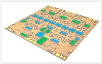
A newly-announced DARPA program is betting that unprecedented on-chip integration of workhorse electronic components, such as transistors and capacitors, with less-familiar magnetic components with names like circulators and isolators, will open an expansive pathway to more capable electromagnetic systems. The Magnetic, Miniaturized, and Monolithically Integrated Components (M3IC), program will orchestrate research into miniaturized magnetic components with a goal of catalyzing chip-based innovations in radar and other radio frequency (RF) systems—and satisfying growing military and civilian demands for new ways to maneuver within the increasingly crowded electromagnetic spectrum.
“Magnetic materials let us access unique physics and functionality that we cannot duplicate with electronic components,” said Dev Palmer, program manager for M3IC (pronounced “M-Cubic”), which is slated for a five-year run with total funding up to $26 million. “M3IC could change the way we design RF circuits and systems.”
The physics and functionality Palmer refers to reside in the principles of electromagnetism, which govern RF signals. It is has been far easier for engineers to design, deploy, and miniaturize RF signal processing in electronics than with magnetic devices, yet some signal processing functions are more effectively achieved by manipulating magnetic fields. One reason for the slow adoption of magnetic components has been the difficulties inherent in miniaturizing and integrating such components directly on chips, alongside electronic circuitry. Among other issues, the magnetic fields that accompany these components can interfere with electronic behavior on chips in unpredictable and undesirable ways. This is why designers of radio, radar, and other RF systems typically segregate the magnetic functions they need off-chip, a limitation that results in bulkier, heavier, and more power-hungry systems compared to the ones that the M3IC program are anticipated to enable.
“M3IC is about distributing the magnetic functionality throughout the circuit instead of pushing it out to the edges,” said Palmer. “It’s about designing and fabricating circuits holistically, so the designer can supercharge state-of-the-art RF electronic circuits with magnetic functionality wherever it is needed, and only where it is needed, in one monolithic chip.”
In particular, Palmer said, seamless co-design and integration of magnetic materials and semiconductors should lead to new generations of more compact microwave monolithically integrated circuits, or MMICs—a class of chips for RF technology developers that offer wider frequency ranges (bandwidth), better stability, and lower power needs than conventional chips.
The new DARPA program is taking on three challenges. The first challenge falls under the category of basic materials science and engineering: to develop techniques for growing and patterning nearly flawless films of magnetic materials (such as hexaferrites and multilayer superlattices with tailorable magnetic properties) on semiconductor wafers while preserving the properties of both the magnetic materials and the semiconductor microcircuitry. The second challenge is to develop the field- and circuit-modeling software necessary for accurate and efficient design of integrated magnetic devices. The third challenge is for engineers to use the new materials and modeling tools to devise and deliver new and improved electromagnetic functionality in smaller, power-efficient packages. By addressing these challenges, the M3IC program will provide the materials and tools necessary to improve the design and performance of existing magnetic components, such as circulators and frequency selective limiters (FSL), and to catalyze innovations of novel, magnetics-enabled, RF-processing technologies.
Frequency selective limiters are especially valuable given the recent proliferation of RF devices in both civilian and military settings, which is increasing the risk of interference. “These limiters, or FSLs, filter out signals that are intentionally or unintentionally trying to jam your reception or damage your receiver,” Palmer explained. “But unlike current receiver protection systems, which work by means of complex sense-analyze-and-actuate loops, FSLs achieve that goal in a much simpler way, as a natural result of their magnetic physics. The ability to produce and integrate miniaturized, power-efficient, interference-management directly onto the billions of RF-involved chips of the future could become a real game changer.”
By integrating the expected advances of the M3IC program into chips endowed with the specialized semiconducting material gallium nitride (GaN), the program also could help provide the military Services with expansive higher-frequency refuge from the overcrowded microwave portion of the spectrum (below 30 Gigahertz). In these already well-subscribed frequency ranges, interfering RF waves can appear as false targets in electronic warfare systems, degrade communications links, and damage sensitive system components. M3IC could ultimately provide the integrated magnetic components necessary to mitigate these problems. By opening the way for a new magneto-electronic design paradigm, the M3IC program also could lead to miniaturized radar systems, higher-capacity channels for transferring data and information, and higher-power RF systems, which could translate into such capabilities as jam-resistance, farther-reaching communications, and more powerful electronic warfare systems.
“By adding magnetics to the MMIC designer’s palette, we hope to open up a whole new design spectrum for RF systems,” Palmer said. “If we get this right, we will bootstrap magnetic component technology to the level of sophistication and integration we enjoy with today’s commercial and military electronics.”
Share on:


Suggested Items
iNEMI Packaging Tech Topic Series: Role of EDA in Advanced Semiconductor Packaging
04/26/2024 | iNEMIAdvanced semiconductor packaging with heterogenous integration has made on-package integration of multiple chips a crucial part of finding alternatives to transistor scaling. Historically, EDA tools for front-end and back-end design have evolved separately; however, design complexity and the increased number of die-to-die or die-to-substrate interconnections has led to the need for EDA tools that can support integration of overall design planning, implementation, and system analysis in a single cockpit.
Cadence, TSMC Collaborate on Wide-Ranging Innovations to Transform System and Semiconductor Design
04/25/2024 | Cadence Design SystemsCadence Design Systems, Inc. and TSMC have extended their longstanding collaboration by announcing a broad range of innovative technology advancements to accelerate design, including developments ranging from 3D-IC and advanced process nodes to design IP and photonics.
Ansys, TSMC Enable a Multiphysics Platform for Optics and Photonics, Addressing Needs of AI, HPC Silicon Systems
04/25/2024 | PRNewswireAnsys announced a collaboration with TSMC on multiphysics software for TSMC's Compact Universal Photonic Engines (COUPE). COUPE is a cutting-edge Silicon Photonics (SiPh) integration system and Co-Packaged Optics platform that mitigates coupling loss while significantly accelerating chip-to-chip and machine-to-machine communication.
Siemens’ Breakthrough Veloce CS Transforms Emulation and Prototyping with Three Novel Products
04/24/2024 | Siemens Digital Industries SoftwareSiemens Digital Industries Software launched the Veloce™ CS hardware-assisted verification and validation system. In a first for the EDA (Electronic Design Automation) industry, Veloce CS incorporates hardware emulation, enterprise prototyping and software prototyping and is built on two highly advanced integrated circuits (ICs) – Siemens’ new, purpose-built Crystal accelerator chip for emulation and the AMD Versal™ Premium VP1902 FPGA adaptive SoC (System-on-a-chip) for enterprise and software prototyping.
Listen Up! The Intricacies of PCB Drilling Detailed in New Podcast Episode
04/25/2024 | I-Connect007In episode 5 of the podcast series, On the Line With: Designing for Reality, Nolan Johnson and Matt Stevenson continue down the manufacturing process, this time focusing on the post-lamination drilling process for PCBs. Matt and Nolan delve into the intricacies of the PCB drilling process, highlighting the importance of hole quality, drill parameters, and design optimization to ensure smooth manufacturing. The conversation covers topics such as drill bit sizes, aspect ratios, vias, challenges in drilling, and ways to enhance efficiency in the drilling department.