


 The Right Approach: I Hear the Train A Comin'
 It’s Only Common Sense: OCCAM—the Time Is Now
 Marcy's Musings: The Growing Industry
Tiny Microchips Enable Extreme Science
July 13, 2016 | NASAEstimated reading time: 2 minutes
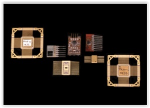
As NASA spacecraft explore deeper into space, onboard computer electronics must not only be smaller and faster, but also be prepared for extreme conditions. A prime example is shown in these images: a family of Application Specific Integrated Circuits, or ASICs, microchips specifically designed to measure the particles in space – the very stuff that can create radiation hazards for satellite computers.
These tiny, radiation-resistant chips play a crucial role in one of the instruments nestled inside the radiation-shielded electronics vault on NASA’s Juno spacecraft – which entered Jupiter’s orbit on July 4. The microchips aboard Juno are part of the Jupiter Energetic Particle Detector Instrument, or JEDI, a cutting-edge instrument that will measure the composition of the immense magnetic system surrounding the planet, called a magnetosphere.
The Application Specific Integrated Circuits, or ASICs, are integral to JEDI’s investigation of unique space environments like that surrounding Jupiter. They will measure the speed, energy and position of particles and photons in space with incredible accuracy.
Credits: NASA’s Goddard Space Flight Center/Joy Ng
The ASICs measure the speed, energy and position of particles and photons in space with time accuracy down to a fraction of a billionth of a second. The largest chip is barely the size of a saltine cracker. Without these chips, satellite electronics would be much heavier and require substantially more shielding and power – potential problems for any satellites traveling into space.
“Before my work, you had electronics that were very big – over two pounds,” said Nikolaos Paschalidis, a space scientist at NASA’s Goddard Space Flight Center in Greenbelt, Maryland. Paschalidis conceived of and first developed ASICs when he worked at the Johns Hopkins Applied Physics Laboratory in Laurel, Maryland. “A great deal of my early work was on miniaturization of space instruments and systems with advanced technologies like electronics onto a microchip.”
Paschalidis is the chief technologist for heliophysics at Goddard. Heliophysics is the study of the sun and how it affects the particles and energy in space. Far from being empty, the space surrounding planets is filled with fast moving particles and a complex electromagnetic system often driven by the sun. Near Jupiter, this system includes intense aurora and giant radiation belts surrounding the gas giant. It’s the job of JEDI, led by Barry Mauk at the Johns Hopkins Applied Physics Laboratory, to observe this complex system.
Better understanding of a planet’s space environment helps us understand how it was formed and continues to evolve. Moreover, it helps us learn more about how to prepare spacecraft to travel through such harsh radiation conditions.
Juno isn’t the first spacecraft to carry these microchips. ASICs have been incorporated in many other NASA missions to study a diverse range of space environments from close to the sun to the heart of Earth’s radiation belts to the edge of the solar system. However, the Juno mission required a significant advance in ASIC performance over prior spaceflight electronics: The Juno ASICs were specially developed to be radiation-hardened, enabling them to withstand the harsh, radiative environment of Jupiter’s magnetosphere where high-energy particles constantly bombard objects and deposit large doses of radiation.
Share on:


Suggested Items
Book Excerpt: The Printed Circuit Assembler’s Guide to... Factory Analytics
04/24/2024 | I-Connect007 Editorial TeamIn our fast-changing, deeply competitive, and margin-tight industry, factory analytics can be the key to unlocking untapped improvements to guarantee a thriving business. On top of that, electronics manufacturers are facing a tremendous burden to do more with less. If you don't already have a copy of this book, what follows is an excerpt from the introduction chapter of 'The Printed Circuit Assembler’s Guide to... Factory Analytics: Unlocking Efficiency Through Data Insights' to whet your appetite.
Listen Up! The Intricacies of PCB Drilling Detailed in New Podcast Episode
04/25/2024 | I-Connect007In episode 5 of the podcast series, On the Line With: Designing for Reality, Nolan Johnson and Matt Stevenson continue down the manufacturing process, this time focusing on the post-lamination drilling process for PCBs. Matt and Nolan delve into the intricacies of the PCB drilling process, highlighting the importance of hole quality, drill parameters, and design optimization to ensure smooth manufacturing. The conversation covers topics such as drill bit sizes, aspect ratios, vias, challenges in drilling, and ways to enhance efficiency in the drilling department.
Elevating PCB Design Engineering With IPC Programs
04/24/2024 | Cory Blaylock, IPCIn a monumental stride for the electronics manufacturing industry, IPC has successfully championed the recognition of the PCB Design Engineer as an official occupation by the U.S. Department of Labor (DOL). This pivotal achievement not only underscores the critical role of PCB design engineers within the technology landscape, but also marks the beginning of a transformative journey toward nurturing a robust, skilled workforce ready to propel our industry into the future.
Winner of The Science Show Rakett 69 Receives Incap Scholarship
04/24/2024 | IncapThe winner of the Rakett 69 science show, Andri Türkson, who stood out as an electronics enthusiast, received a scholarship from Incap Estonia, along with an internship opportunity in Saaremaa.
Alternative Manufacturing Inc. Awarded QML Requalification to IPC J-STD-001 and IPC-A-610
04/24/2024 | IPCIPC's Validation Services Program has awarded an IPC J-STD-001 and IPC-A-610 Qualified Manufacturers Listing (QML) requalification to Alternative Manufacturing Inc (AMI).