


 Flexible Thinking: PCB Designers Still Wanted
 Connect the Dots: Five Best Practices for Designing Flex and Rigid-flex PCBs
 Tim’s Takeaways: Human Ingenuity and the Rigid-flex PCB
Inkjet-printed Liquid Metal Could Bring Wearable Tech, Soft Robotics
April 8, 2015 | Purdue UniversityEstimated reading time: 2 minutes
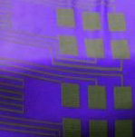
New research shows how inkjet-printing technology can be used to mass-produce electronic circuits made of liquid-metal alloys for "soft robots" and flexible electronics.
Elastic technologies could make possible a new class of pliable robots and stretchable garments that people might wear to interact with computers or for therapeutic purposes. However, new manufacturing techniques must be developed before soft machines become commercially feasible, said Rebecca Kramer, an assistant professor of mechanical engineering at Purdue University.
"We want to create stretchable electronics that might be compatible with soft machines, such as robots that need to squeeze through small spaces, or wearable technologies that aren't restrictive of motion," she said. "Conductors made from liquid metal can stretch and deform without breaking."
A new potential manufacturing approach focuses on harnessing inkjet printing to create devices made of liquid alloys.
"This process now allows us to print flexible and stretchable conductors onto anything, including elastic materials and fabrics," Kramer said.
A research paper about the method will appear on April 18 in the journal Advanced Materials. The paper generally introduces the method, called mechanically sintered gallium-indium nanoparticles, and describes research leading up to the project. It was authored by postdoctoral researcher John William Boley, graduate student Edward L. White and Kramer.
A printable ink is made by dispersing the liquid metal in a non-metallic solvent using ultrasound, which breaks up the bulk liquid metal into nanoparticles. This nanoparticle-filled ink is compatible with inkjet printing.
"Liquid metal in its native form is not inkjet-able," Kramer said. "So what we do is create liquid metal nanoparticles that are small enough to pass through an inkjet nozzle. Sonicating liquid metal in a carrier solvent, such as ethanol, both creates the nanoparticles and disperses them in the solvent. Then we can print the ink onto any substrate. The ethanol evaporates away so we are just left with liquid metal nanoparticles on a surface."
After printing, the nanoparticles must be rejoined by applying light pressure, which renders the material conductive. This step is necessary because the liquid-metal nanoparticles are initially coated with oxidized gallium, which acts as a skin that prevents electrical conductivity.
"But it's a fragile skin, so when you apply pressure it breaks the skin and everything coalesces into one uniform film," Kramer said. "We can do this either by stamping or by dragging something across the surface, such as the sharp edge of a silicon tip."
The approach makes it possible to select which portions to activate depending on particular designs, suggesting that a blank film might be manufactured for a multitude of potential applications.
"We selectively activate what electronics we want to turn on by applying pressure to just those areas," said Kramer, who this year was awarded an Early Career Development award from the National Science Foundation, which supports research to determine how to best develop the liquid-metal ink.
The process could make it possible to rapidly mass-produce large quantities of the film.
Future research will explore how the interaction between the ink and the surface being printed on might be conducive to the production of specific types of devices.
"For example, how do the nanoparticles orient themselves on hydrophobic versus hydrophilic surfaces? How can we formulate the ink and exploit its interaction with a surface to enable self-assembly of the particles?” she said.
The researchers also will study and model how individual particles rupture when pressure is applied, providing information that could allow the manufacture of ultrathin traces and new types of sensors.
Share on:


Suggested Items
Connect the Dots: Designing for Reality—The Pre-Manufacturing Process
05/08/2024 | Matt Stevenson -- Column: Connect the DotsI have been working with Nolan Johnson on a podcast series about designing PCBs for the reality of manufacturing. By sharing lessons learned over a long career in the PCB industry, we hope to shorten learning curves and help designers produce better boards with less hassle and rework. Episode 2 deals with the electronic pre-manufacturing process. Moving from CAD (computer-aided design) to CAM (computer-aided manufacturing) is a key step in PCB manufacturing. CAM turns digital designs into instructions that machines can use to actually build the PCB.
All Flex Solutions Hires Mike Madetzke as Manager of R&D
05/08/2024 | All Flex SolutionsAll Flex Solutions is very pleased to announce that Mike Madetzke has joined their team as their new Manager of Research and Development.
Shane Whiteside of Summit Reflects on Today's PCB Landscape
05/08/2024 | I-Connect007 Editorial TeamSummit Interconnect began as a printed circuit board manufacturing company just eight years ago and has seen impressive growth organically and through acquisition. Summit President and CEO Shane Whiteside takes a few moments to share his thoughts on the growing PCB industry in the United States.
America Projected to Triple Semiconductor Manufacturing Capacity by 2032, the Largest Rate of Growth in the World
05/08/2024 | SIAThe Semiconductor Industry Association (SIA), in partnership with the Boston Consulting Group (BCG), released a report on the global chip supply chain that projects the United States will triple its domestic semiconductor manufacturing capacity from 2022—when the CHIPS and Science Act (CHIPS) was enacted—to 2032.
Coherix Partners with EMU on 'Factory of the Future' Technology Program
05/08/2024 | PRNewswireMichigan-based Coherix is working with Eastern Michigan University (EMU) in Ypsilanti to develop "factory-of-the-future" manufacturing and assembly technology.