


 The Right Approach: I Hear the Train A Comin'
 It’s Only Common Sense: OCCAM—the Time Is Now
 Marcy's Musings: The Growing Industry
Henkel Opens Adhesive Technologies Technology Center in Bridgewater
May 16, 2023 | HenkelEstimated reading time: 2 minutes
Henkel, a global leader in adhesives, sealants and functional coatings has officially opened its Technology Center in Bridgewater, New Jersey. Occupying 70,000 square ft., the center provides a unique and interactive destination for the company's strategic partners and customers. The facility showcases Henkel's entire technology portfolio of adhesives, sealants, functional coatings, and specialty materials and supports an environment for collaboration with customers from over 800 industry segments to develop innovative solutions.
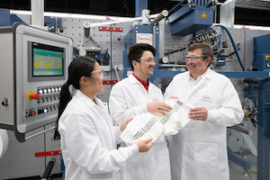
Image caption: At the Technology Center Bridgewater, customers and Henkel experts can tackle production challenges together to find new opportunities. From left: Jocelyn Yuen, Application Engineer; Fielding Water, Application Engineer; Corbett Wallace, Corporate Vice President, Consumer Goods Adhesives
"Innovation is at the core of what we do," said Michael Todd, Vice President of Innovation and New Business Development, Henkel Adhesive Technologies. "The Technology Center Bridgewater is designed to encourage collaboration across the value chain. We have successfully started this concept with the opening of our Inspiration Center Düsseldorf last year and aim to adapt and leverage in core markets for our Adhesive Technologies business such as North America as well."
"The central focus of Adhesive Technologies' innovation activities is developing sustainable solutions for our customers," said Michael Harwell, Vice President of Innovation, Consumer Goods Adhesives. "With the help of digital technologies, many exhibits, and numerous labs, customers from across the U.S., Canada and Mexico can directly experience our innovative and technological power. We're excited to invite customers and partners alike to the facility to work together with us."
The Technology Center features an interactive infinity room that includes a display of Henkel Adhesives Technologies' most innovative solutions in the region. Some of the featured programs include sustainable packaging for consumer goods, sustainable trends in palletizing, smart health solutions with printed electronics for diapers and personal health monitoring, digital solutions for maintenance, repair and operation of manufacturing equipment, and advances in engineered wood building applications.
"Henkel's investment in the center is a testament to its commitment to grow and enhance its market position in the U.S, contributing to profitable growth," added Pernille Olsen, Corporate Vice President, Packaging and Consumer Goods Adhesives. "The Adhesive Technologies' Technology Center in Bridgewater expands on Henkel's leading position in sustainability and innovation by providing a functional, yet inspiring, collaboration space for partners and customers. Through onsite collaboration at the Technology Center, we can fully customize customer interaction to focus on co-innovation and joint value creation."
Henkel Adhesives Technologies employs more than 200 workers at the Bridgewater site. In addition to world class analytical and rheology capabilities, the site supports the Hygiene, Packaging and Labeling, Tissue and Towel, Flexible Packaging, Paper Lamination, EPIX packaging, Pressure Sensitive Tapes, Graphics, Medical and Labels, Engineered Wood, and Furniture and Construction markets.
Share on:


Suggested Items
Warm Windows and Streamlined Skin Patches – IDTechEx Explores Flexible and Printed Electronics
04/26/2024 | IDTechExFlexible and printed electronics can be integrated into cars and homes to create modern aesthetics that are beneficial and easy to use. From luminous car controls to food labels that communicate the quality of food, the uses of this technology are endless and can upgrade many areas of everyday life.
iNEMI Packaging Tech Topic Series: Role of EDA in Advanced Semiconductor Packaging
04/26/2024 | iNEMIAdvanced semiconductor packaging with heterogenous integration has made on-package integration of multiple chips a crucial part of finding alternatives to transistor scaling. Historically, EDA tools for front-end and back-end design have evolved separately; however, design complexity and the increased number of die-to-die or die-to-substrate interconnections has led to the need for EDA tools that can support integration of overall design planning, implementation, and system analysis in a single cockpit.
Koh Young Showcases Award-winning Inspection Solutions at SMTconnect with SmartRep in Hall 4A.225
04/25/2024 | Koh Young TechnologyKoh Young Technology, the industry leader in True 3D measurement-based inspection solutions, will showcase an array of award-winning inspection and measurement solutions at SMTconnect alongside its sales partner, SmartRep, in booth 4A.225 at NürnbergMesse from June 11-13, 2023. The following offers a glimpse into what Koh Young will present at the tradeshow:
Real Time with… IPC APEX EXPO 2024: Plasmatreat: Innovative Surface Preparation Solutions
04/25/2024 | Real Time with...IPC APEX EXPOIn this interview, Editor Nolan Johnson speaks with Hardev Grewal, CEO and president of Plasmatreat, a developer of atmospheric plasma solutions. Plasmatreat uses clean compressed air and electricity to create plasma, offering environmentally friendly methods for surface preparation. Their technology measures plasma density for process optimization and can remove organic micro-contamination. Nolan and Hardev also discuss REDOX-Tool, a new technology for removing metal oxides.
Nanotechnology Market to Surpass $53.51 Billion by 2031
04/25/2024 | PRNewswireSkyQuest projects that the nanotechnology market will attain a value of USD 53.51 billion by 2031, with a CAGR of 36.4% over the forecast period (2024-2031).