


 The Right Approach: I Hear the Train A Comin'
 It’s Only Common Sense: OCCAM—the Time Is Now
 Marcy's Musings: The Growing Industry
Intel Opens Fab 9 in New Mexico
January 25, 2024 | IntelEstimated reading time: 2 minutes
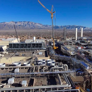
Intel celebrated the opening of Fab 9, its cutting-edge factory in Rio Rancho, New Mexico. The milestone is part of Intel's previously announced $3.5 billion investment to equip its New Mexico operations for the manufacturing of advanced semiconductor packaging technologies, including Intel’s breakthrough 3D packaging technology, Foveros, which offers flexible options for combining multiple chips that are optimized for power, performance and cost.
“Today, we celebrate the opening of Intel’s first high-volume semiconductor operations and the only U.S. factory producing the world’s most advanced packaging solutions at scale. This cutting-edge technology sets Intel apart and gives our customers real advantages in performance, form factor and flexibility in design applications, all within a resilient supply chain. Congratulations to the New Mexico team, the entire Intel family, our suppliers, and contractor partners who collaborate and relentlessly push the boundaries of packaging innovation,” said Keyvan Esfarjani, Intel executive vice president and chief global operations officer.
Intel’s global factory network is a competitive advantage that enables product optimization, improved economies of scale and supply chain resilience. The Fab 9 and Fab 11x facilities in Rio Rancho represent the first operational site for mass production of Intel’s 3D advanced packaging technology. It is also Intel's first co-located high-volume advanced packaging site, marking an end-to-end manufacturing process that creates a more efficient supply chain from demand to final product.
Fab 9 will help fuel the next era of Intel’s innovation in advanced packaging technologies. As the semiconductor industry moves into the heterogeneous era that uses multiple “chiplets” in a package, advanced packaging technologies, such as Foveros and EMIB (embedded multi-die interconnect bridge), offer a faster and more cost-efficient path toward achieving 1 trillion transistors on a chip and extending Moore’s Law beyond 2030.
Foveros, Intel’s 3D advanced packaging technology, is a first-of-its-kind solution that enables the building of processors with compute tiles stacked vertically, rather than side-by-side. It also allows Intel and foundry customers to mix and match compute tiles to optimize cost and power efficiency.
"This investment by Intel underscores New Mexico’s continued dedication to bring manufacturing back home to America," said Gov. Michelle Lujan Grisham. "Intel continues to play a key role in the state’s technology landscape and strengthen our workforce, supporting thousands of New Mexico families.”
The $3.5 billion investment in Rio Rancho has created hundreds of high-tech Intel jobs, more than 3,000 construction jobs and an additional 3,500 jobs across the state.
Share on:


Suggested Items
iNEMI Packaging Tech Topic Series: Role of EDA in Advanced Semiconductor Packaging
04/26/2024 | iNEMIAdvanced semiconductor packaging with heterogenous integration has made on-package integration of multiple chips a crucial part of finding alternatives to transistor scaling. Historically, EDA tools for front-end and back-end design have evolved separately; however, design complexity and the increased number of die-to-die or die-to-substrate interconnections has led to the need for EDA tools that can support integration of overall design planning, implementation, and system analysis in a single cockpit.
IDTechEx Explores the Role of 3D Cu-Cu Hybrid Bonding in Powering Future HPC and AI Products
04/18/2024 | PRNewswireSemiconductor packaging has evolved from traditional 1D PCB levels to cutting-edge 3D hybrid bonding at the wafer level, achieving interconnecting pitches as small as single micrometers and over 1000 GB/s bandwidth. Key parameters, including Power, Performance, Area, and Cost, are crucial considerations
IMAPS & IPC to Host Onshoring Workshop
04/16/2024 | IPCThe International Microelectronics Assembly and Packaging Society (IMAPS) and IPC will host an Onshoring Workshop to discuss ongoing progress and forward-looking strategies to drive the Onshoring Advanced Packaging and Assembly, April 29 – May 1, 2024, in Arlington, Virginia.
Material Insight: The Importance of Standards for the Chip Packaging Industry
04/12/2024 | Dr. Preeya Kuray -- Column: Material InsightI had the great pleasure of recently attending the National Institute of Standards and Technology’s (NIST) CHIPS R&D Chiplets Interfaces Technical Standards Workshop. The purpose was to bring together technical experts across industry and academia to deliberate one of the most pressing technological matters of 2024: chip packaging standards.
Infineon, Amkor Deepen Partnership and Strengthen European Supply Chain for Semiconductor Solutions
04/10/2024 | InfineonInfineon Technologies AG, a leader in power systems and IoT, is strengthening its outsourced backend manufacturing footprint in Europe and announced a multi-year partnership with Amkor Technology, Inc., a leading provider of semiconductor packaging and test services.