


 The Right Approach: I Hear the Train A Comin'
 It’s Only Common Sense: OCCAM—the Time Is Now
 Marcy's Musings: The Growing Industry
HENSOLDT and Nano Dimension Achieve Breakthrough in Electronics 3D Printing
May 19, 2020 | Nano DimensionEstimated reading time: 1 minute
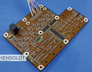
Sensor solutions provider HENSOLDT together with the leading Additively Manufactured Electronics (AME)/Printed Electronics (PE) provider, Nano Dimension, has achieved a major breakthrough on its way to utilizing 3D printing in the development process of high-performance electronics components. Utilizing a newly developed dielectric polymer ink and conductive ink from Nano Dimension, HENSOLDT succeeded in assembling the world-wide first 10-layer printed circuit board (PCB) which carries high-performance electronic structures soldered to both outer sides. Until now, 3D-printed boards could not bear the soldering process necessary for two-sided population of components.
“Military sensor solutions require performance and reliability levels far above those of commercial components.” said HENSOLDT CEO, Thomas Müller. “To have high-density components quickly available with reduced effort by means of 3D printing gives us a competitive edge in the development process of such high-end electronic systems.”
“Nano Dimension’s relationship with HENSOLDT is the type of partnership with customers we are striving for,” commented Yoav Stern, Nano Dimension President and CEO. “Working together and learning from HENSOLDT led us to reach a first-of-its-kind in-depth knowledge of polymer materials applications. Additionally, it guided us in the development of Hi-PEDs (high performance electronic device) that create competitive edges by enabling unique implementations with shortest time to market.”
AMEs are useful to verify a new design and functionality of specialized electronic components before production. AME is a highly agile and individual engineering methodology to prototype a new electronic circuitry. This leads to significant reduction of time and cost in the development process. Furthermore, AME gives a verified and approved design before production starts, leading to higher quality of the final product.
HENSOLDT started working with Nano Dimension’s DragonFly 3D printing system in 2016, in order to examine the possibilities of 3D printing electronics. Last year, HENSOLDT successfully implemented the DragonFly Lights-Out Digital Manufacturing (LDM) printing technology, the industry’s only additive manufacturing platform for round-the-clock 3D printing of electronic circuitry.
Share on:


Suggested Items
Book Excerpt: The Printed Circuit Assembler’s Guide to... Factory Analytics
04/24/2024 | I-Connect007 Editorial TeamIn our fast-changing, deeply competitive, and margin-tight industry, factory analytics can be the key to unlocking untapped improvements to guarantee a thriving business. On top of that, electronics manufacturers are facing a tremendous burden to do more with less. If you don't already have a copy of this book, what follows is an excerpt from the introduction chapter of 'The Printed Circuit Assembler’s Guide to... Factory Analytics: Unlocking Efficiency Through Data Insights' to whet your appetite.
Listen Up! The Intricacies of PCB Drilling Detailed in New Podcast Episode
04/25/2024 | I-Connect007In episode 5 of the podcast series, On the Line With: Designing for Reality, Nolan Johnson and Matt Stevenson continue down the manufacturing process, this time focusing on the post-lamination drilling process for PCBs. Matt and Nolan delve into the intricacies of the PCB drilling process, highlighting the importance of hole quality, drill parameters, and design optimization to ensure smooth manufacturing. The conversation covers topics such as drill bit sizes, aspect ratios, vias, challenges in drilling, and ways to enhance efficiency in the drilling department.
Elevating PCB Design Engineering With IPC Programs
04/24/2024 | Cory Blaylock, IPCIn a monumental stride for the electronics manufacturing industry, IPC has successfully championed the recognition of the PCB Design Engineer as an official occupation by the U.S. Department of Labor (DOL). This pivotal achievement not only underscores the critical role of PCB design engineers within the technology landscape, but also marks the beginning of a transformative journey toward nurturing a robust, skilled workforce ready to propel our industry into the future.
Winner of The Science Show Rakett 69 Receives Incap Scholarship
04/24/2024 | IncapThe winner of the Rakett 69 science show, Andri Türkson, who stood out as an electronics enthusiast, received a scholarship from Incap Estonia, along with an internship opportunity in Saaremaa.
Alternative Manufacturing Inc. Awarded QML Requalification to IPC J-STD-001 and IPC-A-610
04/24/2024 | IPCIPC's Validation Services Program has awarded an IPC J-STD-001 and IPC-A-610 Qualified Manufacturers Listing (QML) requalification to Alternative Manufacturing Inc (AMI).